

ASML Holding NV, one of the world’s leading makers of semiconductor manufacturing equipment, this week said that it had signed an agreement with one of its major U.S.-based customers to deliver at least 15 ASML extreme ultraviolet (EUV) EUV lithography systems. Given the scale of the order it is highly likely that ASML’s customer is Intel Corp.
ASML indicated that the systems will be used to support increased development activity and pilot production of future-generation manufacturing processes. In particular, the owner of the equipment plans to use EUV lithography for multiple processing steps in “future process technology nodes”, but ASML did not reveal which ones. At present it is believed that Intel will use EUV for making chips using 7nm and 5nm process technologies.
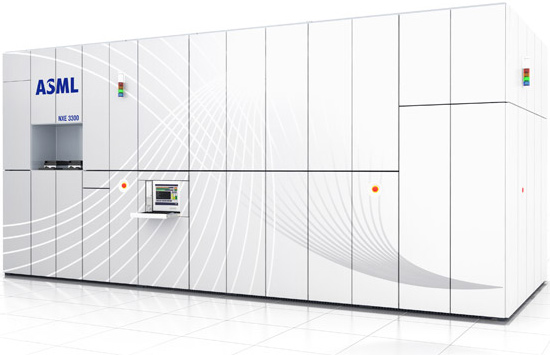
The first two NXE:3350B EUV systems are expected to be delivered before the end of 2015. The new systems will be in addition to the existing EUV development systems already at the customer.
So far ASML has shipped less than ten NXE:3300B EUV test systems to clients. Last year the company began to upgrade light source inside test systems to boost their productivity to 500 wafers per 24 hours. For high-volume manufacturing a wafer scanner should process 1500+ wafers per 24 hours. Previously it was expected that the semiconductor industry would use EUV lithography starting from 2015-2016 and 10nm process technology. Since there are no scanners with proper characteristics today, EUV lithography will only be adopted sometimes in 2017 or later.
Extreme ultraviolet lithography is the leading new patterning technology that allows semiconductor manufacturers to continue scaling down feature sizes of chips. Thanks to 13.5nm wavelength of EUV lasers, it will be possible to “draw” finer elements of chips without using tricky multiple-patterning techniques and implementing additional metal layers that complicate production process and make it more expensive. EUV also promises to bring significant benefits in terms of yield and cycle time.
“EUV is now approaching volume introduction. Long-term EUV planning and EUV ecosystem preparation is greatly supported by this commitment to EUV, kick-starting a new round of innovation in the semiconductor industry,” said Peter Wennink, chief executive officer of ASML. “The commitment extends the planning horizon and increases the confidence in EUV.”
Financial terms were not disclosed, but is the deal is worth hundreds of millions of dollars.
Discuss on our Facebook page, HERE.
KitGuru Says: The order of 15 systems proves that EUV lithography will be used for mass production of chips. The question is when.