Listen to this article 4 min
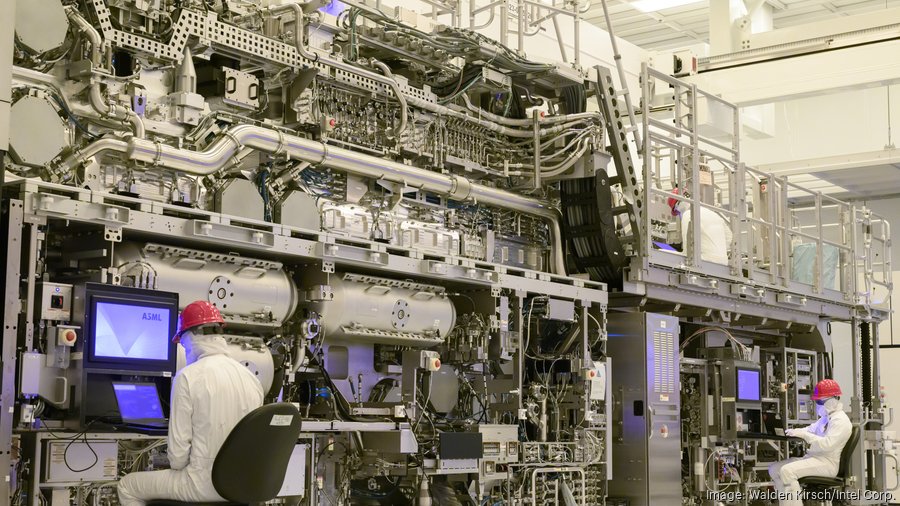
Intel (Nasdaq: INTC) is heralding its embrace in Oregon of cutting-edge semiconductor manufacturing technology — a hulking "$400-ish million" machine with a tennis-court-sized footprint — in a sign of the company's determination to regain global chipmaking dominance.
It's a mission Pat Gelsinger has led since taking over as CEO in 2021.
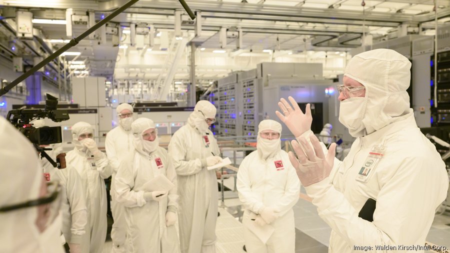
Intel invited a half-dozen media outlets, including the Business Journal, inside its Hillsboro facilities last week to show off the first commercially deployed high-NA EUV system. Offering the rare glimpse of its global R&D nerve center was part of a coordinated media campaign, under wraps until Thursday morning, that carries the claim that Intel is, as it once was, the leader in advancing chip technology.
The formal announcement from Intel on Thursday was that it had completed assembly of the high numerical aperture extreme ultraviolet lithography scanner made by the Dutch company ASML. Used to print ever-smaller patterns onto silicon wafers, it brings the promise of more powerful chips.
"Other technologies continue to advance," said Mark Phillips, Intel's lithography leader. "But this is the most impactful. This is the largest tool in the factory."
Oregon remains a cornerstone for Intel
In broadcasting the high-NA EUV message to the world, Intel was also making a statement that Oregon, where it employs 23,000 people, will remain a cornerstone of its business. There were questions about that a couple of years ago, after the company announced an expansion in Arizona and then a massive new outpost in Ohio. But with high-NA EUV in place and a $36 billion Oregon expansion planned, no one is questioning Intel's commitment.
"This is the center for semiconductor process innovation," Jeff Birdsall, Intel's VP and GM of logic technology development in Oregon, said. He meant not just for Intel, or even the country, but "in the world."
Intel Oregon is a dazzling display of human ingenuity. In its sprawling manufacturing buildings, or fabs, the air is intensively filtered and turned over every two minutes, creating an environment free of the tiniest specks of contaminants. Sealed boxes whiz around on an overhead track system, carrying silicon wafers on a three-to-six-month, 200-mile journey with hundreds of stops at varying machines that build the chips layer by layer.
The high-NA EUV tool isn't one of those stops yet. Engineers from ASML and Intel are continuing to calibrate the machine (ASML employs around 800 people in the area, and says some 250 company engineers will be involved in setting up the high NA tool). Intel said it will begin using it in developing future technology next year, although it doesn't expect chips in the market from high-NA EUV until 2027.
The tool builds on what might be called "standard" EUV that came into industry use late last decade. Intel was a key partner in developing that technology, but integrating it was challenging. So the company tried to push its chips forward without EUV and stumbled in doing so. Meanwhile other manufacturers, led by Taiwan Semiconductor Manufacturing Co. (NYSE: TSM), adopted EUV and sped ahead of Intel in making the most sophisticated chips.
Pat Gelsinger's five nodes in four years
For more than three years, Gelsinger has pushed to catch Intel up. Chips are made on what are called process nodes, a vast collection of steps defined by the ability to increase transistor density. Gelsinger vowed to advance Intel five nodes in four years. That appears well on course. The company released its first chip into the market on a node using EUV in 2023 and expects to have products on the last of the five nodes, 18A, next year.
That will edge it ahead of TSMC, Intel says, and high NA will build on the lead. That could boost Gelsinger's more than $100 billion bid to turn Intel Foundry into a powerhouse, making chips for Intel and other companies.
Investors are hardly fully onboard. Intel shares took a big hit when the company broke out its foundry results for the first time earlier this month, revealing a $7 billion operating loss in 2023. The stock is down about 25% this year. Some analysts are skeptical that the high-NA EUV tool will be efficient enough to pay off. Notably, TSMC hasn't yet announced when it will shift to high NA.
But the Intel on display in Oregon this month was one inspired by Gelsinger, its energetic and indefatigable leader, confident it will get the job done.
"Optimism drives innovation," Birdsall said. "We are operating at the very edge. What drives us forward is that optimism that we will figure it out…. Having Pat come in and having us really commit to that journey became a very strong source of motivation."