Researchers have succeeded in making the first nanoribbons from phosphorene – graphene’s 2D phosphorus cousin. The materials, which can be just one atom thick and under a 100 atoms wide, and made from pure crystalline phosphorus, are theoretically predicted to have a wide range of technologically useful and even exotic properties. The high-quality ribbons produced means that these properties can now be measured and the materials tested in various real-world applications.
Phosphorene, which is also known as few-layer black phosphorus, can be obtained by mechanically cleaving black phosphorus crystals (in the same way that graphene layers are mechanically exfoliated from bulk graphite). Although bulk black phosphorus has been known about for over a century, it is only in the last decade that researchers have tried to isolate single layers of the material.
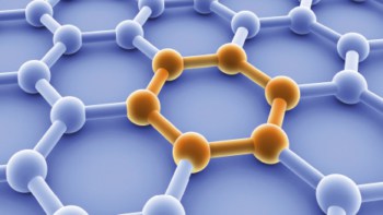
The material’s electronic, thermal and ionic transport properties come from its atomic structure, in which the phosphorus atoms are arranged in corrugated sheets with two different P-P bond lengths.
The researchers, led by Chris Howard of University College London, employed an ion scissoring technique to produce their phosphorene nanoribbons (PNRs). They say they weren’t originally trying to make ribbons but were instead trying out their own method to synthesise various 2D materials in liquids. “In this method, we first take a layered material and insert arrays of alkali metal ions between each layer, which leaves the layers negatively charged,” explains Howard. “The resulting intercalated layered material is then placed in an appropriate solvent and the negatively charged sheets dissolve to form solutions of monolayers.”
Mitch Watts, the study lead author adds: “We were applying this method to black phosphorus crystals and not having much luck. However, after trying several different modifications, we started noticing some ribbon-like fragments in our samples. It took us another three years of hard work and several more adaptations to understand what was happening and to finally be able to produce samples that contained mainly PNRs.”
“Stripes” of ions along phosphorus corrugated channels
Put simply, Howard and colleagues make their PNRs by mixing black phosphorus with lithium ions dissolved in liquid ammonia at -50°C. After 24 hours, they slowly remove the ammonia and replace it with an organic solvent to make a solution of nanoribbons with different sizes. The lithium ions diffuse incredibly fast along the corrugated channels in the black phosphorus crystals, leading to “stripes” of these ions along these channels, explains Howard. The associated high local electron doping causes bond breaking (or cutting) along the stripes and ribbon formation.
“The lithium ions also transfer charge to the ribbons so that when placed in certain solvents, the ribbons can dissolve in a way that is similar to the negatively-charged 2D materials in our previous work.”
The electronic properties of phosphorene lie in between those of the two main classes of 2D materials – that is, graphene and the transition metal dichalcogenides (TMDCs), he adds. Theory calculations predict that the properties of PNRs could surpass those of phosphorene and that their electronic structure, carrier mobilities, optical and mechanical properties can be further tuned by varying the number of layers, the width of the ribbons, edge atom arrangement, roughness of the edges and edge terminating atoms (for example, hydrogen atoms).
Real-world applications
The materials could also possess other interesting properties. These include: an extremely low diffusion barrier for Li, Na and Mg ions along their length, which means they could be useful in high-capacity fast-charging batteries; a high figure of merit for thermoelectrics; and large exciton splitting and favourable bandgap and band positions for photocatalytic water splitting.
Transistors could also benefit thanks to predictions of high charge carrier mobilities in PNRs and fast switching speeds, says Howard. Optoelectronics too, because the materials emit near-infrared light in the 0.2 to 2 eV range.
For applications, the fact that the ribbons can be processed in solution will make a big difference, he adds, since this means that they can be more easily manipulated on the large scale. And because they are flexible, they might be used to make wearable thermoelectric devices.
Exotic states
That is not all: “The materials are also predicted to host a number of exotic states that would be exciting to study as they are at the forefront of several fundamental areas of condensed matter physics,” Howard tells Physics World. “These include: a large singlet-triplet spitting, which could potentially be exploited in quantum information; the spin-dependent Seebeck effect, which could come in useful for low-power consumption technology; topologically-protected edge states; spin-density waves and strain-dependent antiferromagnetism; and half-metallicity for spintronics applications.
“Our technique is the first to produce individual, high-quality PNRs that we can now investigate collectively (for example, using magnetisation measurements) or individually (with a scanning tunnelling microscope or by making them into nanoelectronic devices) to search for these exotic states,” he says.
Phosphorene sees the light
The team, which includes scientists from the University of Bristol, Virginia Commonwealth University and the École Polytechnique Fédérale de Lausanne, is now busy studying the fundamental properties of the PNRs. “We are in particular following up some interesting preliminary work on their optical and electronic properties,” adds Watts. “With our internal collaborators at UCL, we are also working on applications, especially for energy conversion and storage and plan to immediately test the ribbons in some suggested devices – including batteries.”
The researchers, reporting their work in Nature, say they will also be continuing to develop their scanning probe techniques to study the surface of their ribbons.