This article is part of the This Week in PowerBites Library Series.
Salt-Based Battery May Allow Utilities to "Freeze" Excess Power for Use Weeks—or Months—Later
Most folks who garden know the value of canning or freezing the fruits and veggies they grow for consumption during the winter months, but can the same thing be done with wind, solar, and other intermittent renewable-energy sources? Many utilities are already deploying limited amounts of battery storage, often based on the same lithium chemistries used in EVs and personal electronics. However, cost limits their use to propping up the grid for a few hours at a time.
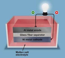
One of the most promising options for storing days, or even weeks, worth of power is an aluminum-nickel molten-salt battery under development at Pacific Northwest National Labs (PNNL).
The battery has several advantages, including the fact that it’s made primarily from inexpensive, Earth-abundant materials. The anode and cathode are solid plates of aluminum and nickel, respectively, which are immersed in a bath of molten-salt electrolyte, with a dash of sulfur added to enhance capacity.
The present battery design can store energy at a materials cost of about $23 per kilowatt-hour (calculated before the recent jump in the cost of nickel), roughly 1/4 the cost of lithium-based chemistries. Meanwhile, the team is exploring the use of iron, which is less expensive, in hopes of bringing the materials cost down to around $6 per kilowatt-hour, roughly 1/15 of the materials cost for today’s lithium-ion batteries.
The molten salt provides the second advantage of loss-free long-term storage. Unlike most other molten-salt batteries, which operate at much higher temperatures, PNNL's electrolyte becomes active at a relatively cool 180°C and solidifies completely somewhere above room temperature.
After charging, the salt electrolyte is allowed to cool and become solid, a state that allows it to retain its stored energy for long periods of time with low levels of self-discharge. Initial tests of a small prototype show that it retained 92% of its capacity during 12 weeks of “cold storage.”
The battery is in its early stages of development, with small prototypes being used to fine-tune the battery's chemistry and construction, and initial results are very promising. The present battery design has a theoretical energy density is 260 watt-hours per kilogram—higher than today’s lead-acid and flow batteries.
It's still unclear if or when the molten-salt battery will be ready to scale to commercial applications. However, if PNNL succeeds, it would open up new options to utilities as they make the transition to carbon-neutral electric grids.
“You can start to envision something like a large battery on a 40-foot tractor-trailer parked at a wind farm,” said co-author Vince Sprenkle, senior strategic advisor at PNNL. “The battery is charged in the spring and then the truck is driven down the road to a substation where the battery is available if needed during the summer heat.”
Additional details are available in PNNL’s article “A Temperature-Based Hibernating Battery” and Scientific American's excellent article “Rechargeable Molten Salt Battery Freezes Energy in Place for Long-Term Storage.”
MDmesh MOSFETs Improve Power Density and Efficiency for Cost-Sensitive Designs
STMicroelectronics’ STPOWER MDmesh M9 and DM9 N-channel superjunction multi-drain silicon power MOSFETs offer improved characteristics that are optimized for switched-mode power supplies (SMPS) in applications from data-center servers and 5G infrastructure to flat-panel televisions.
The first devices to be launched are the 650-V STP65N045M9 and the 600-V STP60N043DM9. Both have very low on-resistance (RDS(on)) per unit area, which maximizes power density and permits compact system dimensions. Each maintains the best maximum RDS(on) (RDS(on)max) in its category, at 45mΩ for the STP65N045M9 and 43mΩ for the STP60N043DM9, according to the company. With very low gate charge (Qg), typically 80 nC at 400-V drain voltage, these devices have the best RDS(on)max x Qg figure of merit (FoM) currently available, says ST.
The gate threshold voltage (VGS(th)), typically 3.7 V for the STP65N045M9 and 4.0 V for STP60N043DM9, minimizes both turn-on and turn-off switching losses compared with the earlier MDmesh M5 and M6/DM6. The MDmesh M9 and DM9 series also feature a very low reverse recovery charge (Qrr) and reverse-recovery time (tRR), which further contribute to improved efficiency and switching performance.
All of ST’s high-voltage MDmesh products incorporate an additional platinum diffusion process that ensures a fast intrinsic body diode. The peak diode-recovery slope (dv/dt) is greater than for earlier processes. All devices belonging to MDmesh DM9 technology are extremely rugged and can withstand dv/dt up to 120 V/ns at 400 V.
The MDmesh M9 and DM9 devices, housed in a TO-220 power package, are already in production. They will be available at distributors by the end of Q2 2022. The STP65N045M9 will be priced from $6.30 for orders of 1,000 pieces. Further standard surface-mount and through-hole package options will be added later in 2022.
For additional product information, go to www.st.com/mdmesh-m9 and www.st.com/mdmesh-dm9.
GaN Power Device Integrates Drive, Protection Features for Medium-to-High-Power Apps
A new 650/800-V-rated GaNFast power IC from Navitas Semiconductor, the NV6169, comes equipped with the company's GaNSense technology. The device is designed to address higher-power applications such as 400- to 1000-W 4K/8K TVs and displays, next-generation gaming systems, 500-W solar microinverters, 1.2-kW data-center SMPS, and up to 4-kW /5-hp motor drives.
With an on-resistance of 45 mW, it offers a 36% reduction in RDS(ON) and 50% more power than prior designs. The NV6169 is housed in an industry-standard, low-profile, low-inductance, 8- × 8-mm PQFN package for high-efficiency, high-density power systems. It’s rated at 650 V for nominal operation plus has an 800-V peak rating for robust operation during transient events. As a truly-integrated power IC, the GaN gate is fully protected; the entire device is rated at an electrostatic-discharge (ESD) specification of 2 kV.
In addition to the higher speed, efficiency, and power density offered by GaN transistors, the company incorporates its GaNSense technology, which integrates power, drive, control, as well as additional autonomous-protection and lossless current sensing to create a single smart power device.
GaNSense also supports rapid short-circuit protection, with a “detect-to-protect” speed of only 30 ns, up to 6X faster than discrete solutions. In motor-drive applications, GaN ICs deliver up to 40% energy savings vs. silicon IGBTs, eliminate 30 external components, and increase system efficiency by 8%.
The NV6169 is available immediately to customers under NDA. Mass-production lead times are currently six to 16 weeks. Simulation models (PSPICE/LTSPICE/SiMetrix), 3D package model (STP), and application note (AN-0016) also are available to designers to optimize next-generation systems.
High-Performance 1200-V Gen-4 SiC FETs Deliver Best-of-Breed Figures of Merit
Qorvo's recently acquired United SiC group announced a next-generation series of 1200-V silicon-carbide (SiC) FETs that offer even better on-resistance-related figures of merit (FoM) than its industry-leading Gen-3 devices. The new UF4C/SC series of Gen-4 SiC FETs were developed to address the requirements of mainstream 800-V bus architectures in onboard chargers for electric vehicles, industrial battery chargers, industrial power supplies, and dc-dc solar inverters. They’re also well-suited for welding machines, uninterruptible power supplies, and induction heating applications.
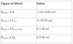
The advanced vertical trench device structure developed by Qorvo gives the new devices extremely low RDS(on) for a given die area, enabling a significant reduction in die size for a given power rating, ranging from 23 to 70 mΩ. Their reduced capacitance and switching losses give them other industry-leading FoM values that translate into high performance in both hard switching (i.e., active front end etc.) and soft switching (i.e., isolated DC/DC converters):
As with the rest of Gen-4 portfolio, the new 1200-V FETs can be easily driven with a 0- to 12- or 0- to 15-V gate drive. With a ±20-V VGS,Max and a high threshold voltage (4.8 V), these SiC FETs offer plenty of gate-voltage design and noise margin and are compatible with Si or SiC gate-drive voltages. The 1200-V FETs offer an excellent integral diode, with superior forward voltage (1.0 to 1.5 V typically) and low reverse-recovery charge (QRR).
Advanced Thermal Performance
To take full advantage of their ultra-low specific on-resistance, the new SiC FETs employ an advanced silver-sinter die-attach process that provides best in-class thermal resistance, Rth, j-c. This, combined with the low RDS(on) enables the use of a smaller die for a given power rating, along with the resulting lower capacitance and reduced switching losses.
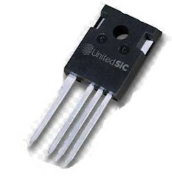
All RDS(on) options (23, 30, 53 and 70 mΩ) are offered in the industry-standard 4-lead Kelvin-source TO-247 package, providing cleaner switching at higher performance levels.
The 53- and 70-mΩ devices also come in the TO-247 3-lead package. This series of parts has excellent reliability, based on the well-managed thermal performance, which is a result of an advanced silver-sinter die-attach and advanced wafer-thinning process.
Design Support
Designing with the 1200-V SiC FETs is simplified thanks to their inclusion in FET-Jet Calculator. The free online design tool allows for instant evaluation of efficiency, component losses, and junction temperature rise of devices used in a wide variety of ac-dc and isolated/non-isolated dc-dc converter topologies.
Pricing (1,000-up, FOB USA) for the new SiC FETs ranges from $5.71 for the UF4C120070K3S, to $14.14 for the UF4SC120023K4S. All devices are available from authorized distributors.
Hybrid Inductive Wireless Power System Supplies up to 40 W to Small IoT Devices
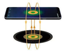
Powermat Technologies released its new Powermat PMT 100 Wireless Power Solution, which is designed to meet the needs of small medical, lifestyle, and smart-home Internet of Things (IoT) devices. The Powermat PMT 100 provides higher performance levels and a straightforward user experience at a price point that makes it practical for large-scale deployment.
The PMT 100 receiver is designed for small-form-factor IoT devices for wireless power and charging, supporting battery-charging functionality and smart battery interfaces. With no receiver-based microcontroller and minimal peripheral components, the Powermat PMT 100 supports the design and development of smaller, more discreet portable products and reduces overall wireless power implementation costs by up to 50%.
Powermat PMT 100 uses Powermat's SmartInductive Technology, which is based on magnetic induction but allows for a broader scope of capabilities than traditional magnetic induction solutions. The technology is actually a hybrid solution that combines the best characteristics of inductive wireless charging and resonance. Thus, it can transmit more power, offer more freedom of positioning, and provide longer ranges between wireless power transmitters and receivers. In addition, SmartInductive designs frequently enjoy lower implementation costs than competing technologies.
Powermat PMT 100 Wireless Power Solution Key Features
- Power range:
- Receiver max power output: 40 W
- Receiver max voltage: 30 V
- Max current: 2 A
- Extremely small PCBA enabling product miniaturization
- Coil support:
- Litz wire or PCB coil
- Coil diameter ≥ 10 mm
- Easy drop and charge solutions for increased misalignment and angular device placement
- Foreign object detection (FOD)
- Battering charging and support of smart battery interface
- Cost-saving solution—up to 50% cost reduction in comparison to standard wireless power receivers
- Powermat transmitter solution compatible
Click here for additional information on the Powermat PMT 100 Wireless Power Solution
Automotive-Qualified IGBT/SiC Module Driver Family Targets Bus, Truck, and Con-Ag EVs
Power Integrations announced its SCALE EV family of ASIL B/C-rated gate-driver boards for Infineon EconoDUAL modules. Suitable for original, clone, and new SiC variants, the driver targets high-power automotive and traction inverters for EV, hybrid, and fuel-cell vehicles, including buses and trucks as well as construction, mining, and agricultural equipment.
SCALE EV board-level gate drivers incorporate two reinforced gate-drive channels, associated power supplies, and monitoring telemetry. The new boards are automotive-qualified and ASIL B certified, enabling implementation of ASIL C traction-inverter designs. The first SCALE EV family member to be released is the 2SP0215F2Q0C, designed for the EconoDUAL 900-A, 1200-V IGBT half-bridge module.
The highly integrated driver ICs reduce component count, enabling the entire driver board, including gate power, to fit onto the outline of the power module—yet it still provides the spacing necessary for reinforced isolation according to the IEC 60664 standard. The ASIC package provides 11.4 mm of creepage and clearance, specifically designed to meet the requirements for 800‑V vehicle system voltages.
Input and output lines to the system microcontroller are connected via two independent on-board connectors to meet functional-safety requirements. A single 5-V supply per channel is required, with other isolated voltages being generated on the board itself.
The SCALE EV gate-driver family, rated at 1200 V for 400- and 800-V systems, supports both silicon-carbide (SiC) MOSFETs and silicon IGBTs. The design carries a 5,500-meter altitude rating and is optionally available with conformal coating for technical cleanliness requirements.
A wide range of protection provisions are incorporated, including active short-circuit; active discharge of connected dc-link capacitor; overvoltage limitation via active gate control; diagnostic functions such as gate monitoring, signal transmission monitoring, and on-chip temperature monitoring; and short-circuit and overcurrent response of less than 1 µs for SiC MOSFETs and less than 3 µs for IGBTs.
Availability & Resources
Samples of the 2SP02152FQ are available now, with full production release in the fourth quarter of 2022. Pricing starts at $200 each for 100-piece quantities.
Support materials for SCALE EV include the datasheet, pressFIT tool CAD design, the RDHP-2250Q adapter breakout board, and PC-based software. To access the support materials, and view a brief video overview of SCALE EV, visit https://www.power.com/products/scale-ev.
TOLL-Packaged 650-V SiC MOSFET Enables Smaller, Cooler-Running Designs
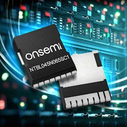
The first TO-Leadless (TOLL) packaged SiC MOSFET was announced at PCIM Europe by onsemi. The transistor addresses the rapidly growing need for high-performance switching devices that accommodate high-power-density designs. Until recently, SiC devices had been primarily supplied in D2PAK 7-lead packages, which required significantly more space.
With a footprint of just 9.90 × 11.68 mm, the TOLL package offers 30% savings in PCB area over a D2PAK package. And at a profile of just 2.30 mm, it occupies 60% less volume than a D2PAK.
In addition to its smaller size, the TOLL package features better thermal performance and lower package inductance (2 nH) than a D2PAK 7-lead, according to onsemi. Its Kelvin-source configuration ensures lower gate noise and lower switching losses, including a 60% reduction in turn-on loss (EON) when compared to a device without a Kelvin configuration. This ensures that efficiency and power density will significantly improve in challenging power designs, as well as improve EMI and simplify PCB design.
The first SiC MOSFET to be offered in the TOLL package is the NTBL045N065SC1, which is intended for demanding applications including switch-mode power supplies (SMPS), server and telecommunication power supplies, solar inverters, uninterruptible power supplies (UPS), and energy storage. The device is suitable for designs that must meet the most challenging efficiency standards, such as ErP and 80 PLUS Titanium.
The NTBL045N065SC1 has a VDSS rating of 650 V with a typical RDS(on) of just 33 mΩ and a maximum drain current (ID) of 73 A. Based on wide-bandgap (WBG) SiC technology, the device has a maximum operating temperature of 175°C and ultra-low gate charge (QG(tot) = 105 nC) that significantly reduces switching losses. In addition, the TOLL package is MSL 1 (moisture sensitivity level 1) rated—and guaranteed—to ensure low failure rates in mass production.
Moreover, onsemi offers automotive-grade devices with TO-247 3 leads, 4 leads, and D2PAK 7 leads packages.
2-kV SiC FETs Deliver Simple, High-Power-Density Solutions for 1,500-V Applications
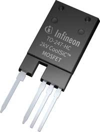
To support the growing number of applications moving to 1,500-VDC operating voltages, Infineon Technologies introduced several high-voltage CoolSiC devices intended to support next-generation applications like photovoltaic, EV charging, and energy-storage systems. The new products overcome many of the challenges associated with 1500-VDC-based systems, such as the complexity and cost of the multi-level switch topologies normally required to achieve fast switching at a high dc voltage.
The new members of the CoolSiC portfolio include 2-kV SiC MOSFETs and a 2-kV SiC diode. The SiC MOSFETs combine low RDS(on), low-switching losses, and high-blocking voltage. Despite their higher operating voltages, the devices still support the CoolSiC family's full extended gate voltage range, leading to simpler, easier designs. In addition, their body diode is sufficiently rugged to support hard switching and offers 1/10th the FIT rate caused by cosmic rays, when compared to 1,700-V SiC MOSFETs.
To complement these devices, Infineon offers a range of EiceDRIVER gate drivers with functional isolation of up to 2.3 kV.
Availability
Samples of EasyPACK 3B and 62-mm modules that integrate the 2 kV CoolSiC MOSFETs are available now, with discrete components sampling by the end of 2022. The 3B module (DF4-19MR20W3M1HF_B11) contains four boost circuits and acts as the MPPT stage of a 1,500-V PV string inverter. Production is planned for Q3 2022, with the 62-mm module in half-bridge configuration (3, 4, 6 mΩ) to follow in Q4 2022. Discrete samples of the 2-kV devices housed in a new high-voltage TO247-PLUS package will be offered by the end of 2022.
Additional information is available at www.infineon.com/CoolSiC.
Read more articles in the This Week in PowerBites Library Series.

