Dec 4 2020
According to scientists from the University of Michigan, the University of Regensburg, and the University of Marburg, an innovative tool that uses light to plot the electronic structures of crystals could demonstrate the potential of emerging quantum materials and may lead to the development of next-generation quantum computers and energy technologies.
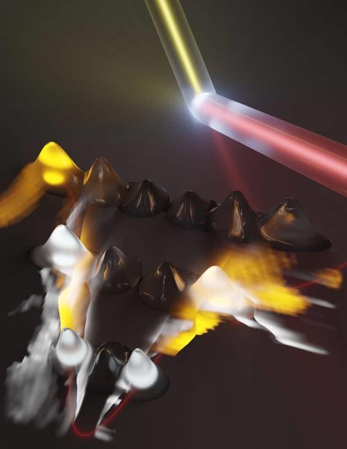 The electrons absorb laser light and set up “momentum combs” (the hills) spanning the energy valleys within the material (the red line). When the electrons have an energy allowed by the quantum mechanical structure of the material—and also touch the edge of the valley—they emit light. This is why some teeth of the combs are bright and some are dark. By measuring the emitted light and precisely locating its source, the researchers mapped out the energy valleys in a 2D crystal of tungsten diselenide. Image Credit: Markus Borsch, Quantum Science Theory Lab, University of Michigan.
An article on this latest study has been published in the Science journal. The new tool can be used in artificial photosynthesis, solar cells, and LED lights.
Quantum materials could have an impact way beyond quantum computing. If you optimize quantum properties right, you can get 100% efficiency for light absorption.
Mackillo Kira, Professor of Electrical Engineering and Computer Science, University of Michigan
Professor Kira headed the theory side of the latest research work.
Solar cells based on silicon material are already turning out to be the most affordable form of electricity, even though their conversion efficiency from sunlight to electricity is quite low, that is, around 30%.
But emerging “2D” semiconductors containing a single crystal layer may do that conversion work relatively better—possibly utilizing up to 100% of the solar light. These semiconductors may also increase quantum computing to room temperatures from the near-absolute-zero machines showcased to date.
New quantum materials are now being discovered at a faster pace than ever. By simply stacking such layers one on top of the other under variable twist angles, and with a wide selection of materials, scientists can now create artificial solids with truly unprecedented properties.
Rupert Huber, Professor of Physics, University of Regensburg
Professor Huber had supervised the experimental study.
The potential to plot such characteristics down to the atoms could help simplify the method of developing materials that have the right quantum structures. However, such ultrathin materials are relatively messier and smaller when compared to the previous crystals, and the ancient analysis techniques definitely do not work. But now, 2D materials can be quantified using the novel laser-based technique at room pressure and temperature.
The quantifiable operations involve procedures that are crucial to optically driven quantum computing, lasers, and solar cells. In essence, electrons emerge between a “ground state,” in which they cannot move freely, and states in the “conduction band” of the semiconductor, in which they can move freely through space. They perform this activity by absorbing and discharging the light.
The quantum mapping techniques make use of a 100-femtosecond (that is, 100 quadrillionths of a second) pulse of red laser light to burst electrons from the ground state and into the conduction band. These electrons are subsequently bombarded with a second pulse of infrared light. This forces them such that they move up and down an energy “valley” in the conduction band, somewhat like skateboarders in a halfpipe.
Using the dual wave/particle nature of electrons, the researchers produced a standing wave pattern that appears similar to a comb. They observed that when the peak of this electron comb overlaps with the band structure of the material—that is, its quantum structure—electrons tend to produce light strongly. That strong emission of light, together with the narrow width of the comb lines, allowed the researchers to generate an extremely sharp picture, which they dubbed super-resolution.
By integrating that accurate location data with the frequency of the light, the researchers were able to plot the band structure of tungsten diselenide—the 2D semiconductor. Besides that, they could get a read on the orbital angular momentum of each electron by the way the front of the light wave twisted in space.
Exploiting the orbital angular momentum of an electron, called a pseudospin, offers a promising method for processing and storing quantum data.
In the case of tungsten diselenide, the orbital angular momentum detects which of the two different “valleys” is occupied by an electron. The messages sent out by the electrons can show scientists which valley is occupied by the electron, the distance between the two valleys, and how the landscape of that valley actually looks like—all of which are the main elements required to develop novel semiconductor-based quantum devices.
For example, when the researchers applied the laser to force the electrons up the side of one valley until they collapsed into the other, the electrons also produced light at that drop point. That light provides clues about the height of the ridge between the valleys as well as their depths. Armed with this kind of data, investigators can find out how the material would fare for a wide range of purposes.
This study was financially supported by the German Research Foundation, the U-M College of Engineering Blue Sky Research Program, and the Army Research Office.
Journal Reference:
Borsch, M., et al. (2020) Super-resolution lightwave tomography of electronic bands in quantum materials. Science. doi.org/10.1126/science.abe2112.
Source: https://ece.engin.umich.edu/