Memristors have been — so far — mostly a solution looking for a problem. However, researchers at the University of Michigan are claiming the first memristor-based programmable computer that has the potential to make AI applications more efficient and faster.
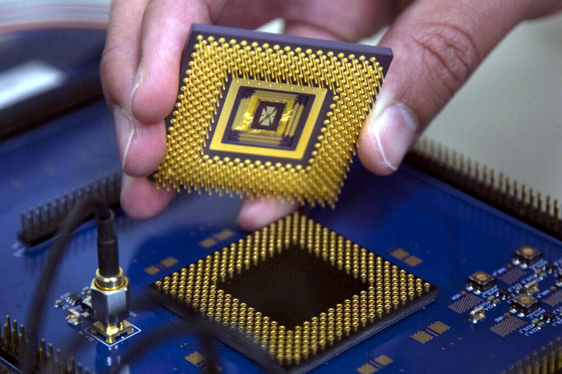
Because memristors have a memory, they can accumulate data in a way that is common for — among other things — neural networks. The chip has both an array of nearly 6,000 memristors, a crossbar array, along with analog to digital and digital to analog converters. In fact, there are 486 DACs and 162 ADCs along with an OpenRISC processor.
According to the paper, the chip turned in 188 billion operations per second per watt while consuming about 300 mW of power. This includes power consumption attributable to the 180 nM CMOS technology, which is not even close to cutting edge. Newer technology would drive the chip’s performance even higher.
By analogy, you can consider a memristor accumulator as a potentiometer that gets twisted a little more with each input. The final position of the potentiometer indicates the sum of the inputs. This kind of technique has been of great interest as CPU power is becoming harder to increase. If you can do processing in memory instead of the CPU, you can achieve great performance, in theory, since you don’t have to transfer memory to a processing unit, do the computation, and then transfer back to memory.
This reminded us of how we saw memristors solving equations although that wasn’t as integrated as this chip. While some people claim that memristors are a new type of fundamental component, there are those that disagree.


” If you can do processing in memory instead of the CPU, you can achieve great performance, in theory, since you don’t have to transfer memory to a processing unit, do the computation, and then transfer back to memory.”
Don’t remember the name, but the idea is actually old. Technology however wasn’t ready.
Different versions have different names but PIM (Processor In Memory) was a popular name once.
“the chip turned in 188 billion operations per second per watt while consuming about 300 mW of power.”
Here it is a great question what type of “operation” we are talking about. If the paper misapplies it to “the resistor changed value”, then this number isn’t at all surprising. If they apply it as “it did all the needed steps to act as a neuron.” then it is more impressive. Though, this isn’t my field of knowledge.
(An operation typically contains more then one instruction, so compared to Instructions per second, OPS will nearly always be a lower number. And since changing value of the memresistor is its most basic instruction, its on par with add/subtract, then we shouldn’t really apply the term “operation” to it. If looking at this from the perspective of comparing computing architectures.)
Though, I do find this sentence “funny”: “This includes power consumption attributable to the 180 nM CMOS technology, which is not even close to cutting edge. Newer technology would drive the chip’s performance even higher.”
First of, the obvious “nM” should be “nm”. Meter is always expressed with a lower case m, even at the start of a sentence, by convention of how to write SI units.
Secondly, the power consumption of CMOS logic is dependent on far more factors then the manufacturing node itself.
The power consumption of a CMOS cell is most greatly impacted by intrinsic capacitance of the transistors and surrounding wiring, and the needed drive voltages for it to reach stable operation. Not to mention how long in stays in the region where both transistors are conducting and the on/off resistance of the transistor. (Switching speed I’ll get to later.)
The manufacturing node most greatly impacts the total number of transistors one can fit in a given area. One can also use a smaller manufacturing node to build more complex transistor structures, as to lower on/off resistance, ensure that only one transistor is on at a time, among other things.
And for everyone thinking, “But a smaller transistor will have less capacitance and lower drive voltages. And thereby we can have higher switching speeds!”
Lower drive voltage means thinner gate “oxide” (it isn’t always silicone dioxide), this thinner gate insulation will thereby have higher capacitance for a given area. Secondly, if we make the gate oxide thin enough, we might need to switch to other materials that have higher break down voltages. These sometimes also make for better capacitors yet again… Do note, sometimes one doesn’t have a choice, semiconductors hates most materials and will usually stop working if contaminated. So the insulator needs to be compatible.
(Reason for why we need high breakdown voltages is due to the fact that we need a certain minimum Vgs voltage for it to survive signal level voltages, noise, etc. And the turn on voltage doesn’t really get linearly effected with a change in insulator thickness. Not to mention the good old quantum tunneling wanting to turn the thing into something between a FET and a BJT device, so lots of fun. (it mostly gives you the worse of both worlds…))
In terms of switching speeds, it is more dependent on the choice of semiconductors, then on the size of the transistor. It is also effected by a few geometrical factors as well. A transistor doped into the surface of a silicone wafer will have different properties compared to a fin based transistor, and so forth. But charging a gate faster will though usually make it respond faster, but eventually the time needed to form the conductive channel is greater then the time needed to charge the gate, making it a very mute point in trying to charge the gate even faster. And what determiners the time needed to form the conductive channel? Well, mostly the properties of the semiconductor, the makeup of the depletion region, and the voltage applied at the gate.
Then one can go into the limitations of production equipment, etc… Since yes, sometimes one simply can’t build certain features on the smaller node. (but this is not usually the case unless one sits down at sub 30-22 nm node.) Or the fact that I so far haven’t even mentioned the analog performance/linearity of the transistors and how that can get effected by lowering the manufacturing node. So for a chip with “486 DACs and 162 ADCs” then it also has to take into consideration. Not to mention the requirements of the memresistors themselves. So they have probably picked wisely what node they want to work at. (After all, it isn’t like one tosses a design into any random node just to get it produced.)
In the end, a smaller manufacturing node isn’t intrinsically better then a bigger one. Though that doesn’t mean one can’t shrink the design, either for a die shrink, or to fit more onto it, or make more complicated transistor designs. If this node change comes with performance/efficiency gains is though a question that isn’t answered by looking at the manufacturing node alone, more information is needed.
Therefor the statement “[… 180 nM CMOS technology, which is not even close to cutting edge. Newer technology would drive the chip’s performance even higher.” is fairly bogus, since most newer technology used in it wouldn’t be expressed by simply looking at the “180 nm” part of the manufacturing process. Intel at least were “smart” in adding a “+” sign to their 14nm node, four or so times over…. (but considering just the improvements in the 48nm node, it would likely have 20+ “+”s today, not to mention other larger manufacturing nodes.)
The colleague nicely explained the editor’s issues in practice. I also have this opinion :)
On Hackaday, it’s always great to see a post about one lone person, with no funding making something in their garage–no wait! Oh well.
The memsistor was quite the buzzword. I would rather some companies spend time working on cheaper static RAM, so we can stop throwing out all of our “cheap” memory to buy new RAM that’s marginally faster. Meanwhile, the branch-prediction attacks continue, and multicore processors begin to feel the RAM bottleneck.
I do have to agree that memresistors is a fair bit of a buzzword, mostly a solution looking for a problem.
Though, the reason static memory is more expensive then DRAM is simply due to the fact that it is roughly 4 times more resource intensive in terms of transistor count.
But there is more nuance to why DRAM is “slow” compared to SRAM. And changing the system memory in a computer to SRAM isn’t honestly going to do much, due to a slew of other reasons.
To name a few:
DDR, DDR2, DDR3, DDR4 and even DDR5 are all using a 64 bit parallel buss. Parallel buses tends to be sensitive to any skews in arrival times, making higher bus clock speeds usually end with instability. (IDE (aka Parallel-ATA) partly got “abandoned” due to this.) A solution system memory makers could implement is simply to use less wide memory buses. Like 16 bit instead of 64 bit and then have 4 times as many buses. (Timing skews can still happen, but at least there is 1/4 as many bits for it to happen on.) Another improvement is to make the buss full duplex, instead of bidirectional as it currently is.
Caching, without it, the CPU cores would be more memory starved then ever. Due to cache memory bandwidth usually being superior to that of any external memory buses. It is also closer to the cores, and has a lot lower access latency. Downside, we need to check if it contains the contents we are after, only after this check we can stroll out to main RAM and fetch it there. This adds a lot of latency if the cache doesn’t have what we are looking for, this is called a cache miss. A solution for some applications is to exclusively use scratch pad memory instead. (But elusively using scratchpad would toss backwards compatibility down the drain, performance wise that is.)
Then there also is the good old signal propagation speed, it takes time sending signals across the board, this is also why a full duplex buss would be advantageous.
And lastly, the memory clock and the core clock are separate, they are usually not remotely similar, aren’t really phase locked to each other. This means we need to buffer data between the clock domains, this typically takes more then a whole clock cycle of the lower frequency clock. A solution would be to run the core clock and the memory clock on the same frequency, and keep them phase locked as well. Downside, clock boosting is then a thing of the past….
So a switch to SRAM as system memory would do next to nothing. Since most systems are already bottleneck when it comes to bandwidth due to timing skews on the memory buss, and latency wise due to cache misses.
A simpler solution would be to make better prefetching systems (probably also add machine code level hints for that system, so that a compiler can make things more obvious), add more cache (typically expensive), and also add more memory buses (a memory buss needs around 200-250 pins on the socket).
In terms of pins on the socket 200-250 pins might not seem like much. But then there is a few hundred pins for power, a few hundred more for PCIe, among other things. Though the AM4 socket has pins for a USB/SATA hub occupying about enough pins for a third memory channel and some more PCIe lanes, since everyone has 5 HDDs and are in need of a few USB ports too…. Not like the chipset has enough of them already. (I would have gladly taken a third DDR4 channel and some additional PCIe lanes instead of the USB/SATA hub….)
Actually the USB/SATA on the AM4 CPU are using the same SERDES as their PCIe. I think they used those in PCIe mode on Epyc.
Individually the SRAM cells are much faster than DRAM, but when you hook them up in a large array you would more complex address decoding and much larger cap load for the busses. Ever wonder why L1 cache is smaller than L2 and L2 than L3 etc. Each size up, the memory get slower. They would slow down quite a lot when you scale them up to DRAM density.
Yes, large SRAM arrays also tend to suffer from large amounts of trace capacitance.
This can be alleviated by the use of many smaller arrays, though at the expense of more complicated buss and address systems. Also making the SRAM even more expensive due to it needing more transistors….
Though, I am of the opinion that an additional DDR4 memory channel would be far more useful compared to a USB/SATA controller, in general use. Especially with AMD’s recent addition of PCIe 4.0