Nov 5 2019
Contemporary construction is always a precision endeavor. As such, builders have to use components such as rivets of a particular size or beams of a required composition to fulfill specific standards.
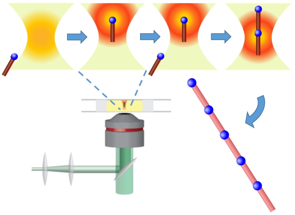 Focused laser light generates an optical “tractor beam,” which can manipulate and orient semiconductor nanorods (red) with metal tips (blue) in an organic solvent solution. The energy from the laser superheats the metallic tip of the trapped nanorod, allowing the aligned nanorods to be welded together end-to-end in a solution-based “nanosoldering” process. (Image credit: Vincent Holmberg/Matthew Crane/Elena Pandres/Peter Pauzauskie)
The building sector depends on manufacturers to produce these components in a reliable and reproducible way to build sound skyscrapers and secure bridges.
Now, one can envision a construction at a smaller scale, or more precisely, the nanoscale—that is, less than 1/100th the thickness of a piece of paper. Researchers are working at this scale to create potentially innovative technologies in areas like quantum computing.
The nanoscale is also the scale where conventional fabrication techniques will not work at all. The typical tools, including the miniaturized ones, are too corrosive and too large to reproducibly produce components at the nanoscale.
At the University of Washington (UW), scientists have devised a new technique that can make it possible to realize reproducible manufacturing at the nanoscale. The researchers modified a light-based technology—called optical tweezers or optical traps—that is extensively used in biology.
Their aim is to make these optical tweezers to work in a water-free liquid setting of carbon-rich organic solvents, allowing new, promising applications. The study has been published on October 30th, 2019, in the Nature Communications journal.
According to the researchers, the optical tweezers behave as a light-based “tractor beam” that can accurately organize nanoscale semiconductor materials into larger structures. The researchers used the optical tweezers to capture materials that are almost a billion times shorter than a meter. This approach is different from the tractor beams of science fiction, which capture spaceships.
This is a new approach to nanoscale manufacturing. There are no chamber surfaces involved in the manufacturing process, which minimizes the formation of strain or other defects. All of the components are suspended in solution, and we can control the size and shape of the nanostructure as it is assembled piece by piece.
Peter Pauzauskie, Associate Professor, Materials Science and Engineering, University of Washington
Pauzauskie is the co-senior author of the study and a faculty member at the Molecular Engineering & Sciences Institute and the Institute for Nano-engineered Systems. He is also a senior scientist at the Pacific Northwest National Laboratory.
“Using this technique in an organic solvent allows us to work with components that would otherwise degrade or corrode on contact with water or air,” stated Vincent Holmberg, co-senior author and assistant professor of chemical engineering at the UW. Holmberg is also a faculty member in the Clean Energy Institute and the Molecular Engineering & Sciences Institute.
Holmberg continued, “Organic solvents also help us to superheat the material we’re working with, allowing us to control material transformations and drive chemistry.”
To exhibit the potential of this method, the team utilized the optical tweezers to construct a unique nanowire heterostructure—a nanowire containing distinct sections, which, in turn, contain different materials.
The preliminary materials used to build the nanowire heterostructure included shorter “nanorods” of crystalline germanium, each measuring only tens of nanometers in diameter and a few hundred nanometers long—or approximately 5000 times thinner than a single strand of human hair. Each germanium nanorod is covered with a metallic bismuth nanocrystal.
Then, using the light-based “tractor beam”, the scientists grabbed one of the germanium nanorods. Moreover, energy from the beam considerably heats up the nanorod and thus melts the bismuth cap. The researchers then guided a second nanorod into the light-based “tractor beam” and—using the molten bismuth cap provided at the end—fused them end-to-end.
The scientists were able to perform the process again until they had organized a patterned nanowire heterostructure that has repeating semiconductor-metal junctions. These junctions were 5 to 10 times longer than the separate building blocks.
We’ve taken to calling this optically-oriented assembly process ‘photonic nanosoldering’—essentially soldering two components together at the nanoscale using light.
Vincent Holmberg, Assistant Professor, Department of Chemical Engineering, University of Washington
Nanowires containing junctions between materials—like the germanium-bismuth junctions produced by the UW research team—may ultimately pave the way for producing topological qubits for use in quantum computing.
The light-based tractor beam is essentially a highly focused laser that produces a type of optical trap, a technique that won the Nobel Prize and was first developed by Arthur Ashkin in the 1970s. So far, optical traps have been utilized almost entirely in vacuum- or water-based settings. The research teams of Pauzauskie and Holmberg modified optical trapping to work in the more volatile setting of organic solvents.
“Generating a stable optical trap in any type of environment is a delicate balancing act of forces, and we were lucky to have two very talented graduate students working together on this project,” added Holmberg.
The photons that constitute the laser beam create a force on objects in the close vicinity of the optical trap. The properties of the laser can then be adjusted so that the force produced can either release or trap an object, whether it is a longer nanowire or a single germanium nanorod.
This is the kind of precision needed for reliable, reproducible nanofabrication methods, without chaotic interactions with other surfaces or materials that can introduce defects or strain into nanomaterials.
Peter Pauzauskie, Associate Professor, Materials Science and Engineering, University of Washington
According to the scientists, their nanosoldering method can facilitate additive manufacturing of nanoscale structures with different groups of materials for other kinds of applications.
“We hope that this demonstration results in researchers using optical trapping for the manipulation and assembly of a wider set of nanoscale materials, irrespective of whether or not those materials happen to be compatible with water,” stated Holmberg.
The paper’s co-lead authors are Elena Pandres, a UW graduate student in chemical engineering, and also Matthew Crane, a UW doctoral graduate and now a postdoctoral researcher in the UW Department of Chemistry. The paper’s co-author is E. James Davis, a UW professor emeritus of chemical engineering.
The National Science Foundation, the UW Molecular Engineering Materials Center, the UW Molecular Engineering & Sciences Institute, the UW Institute for Nano-engineered Systems, the UW Clean Energy Institute, the State of Washington, the Washington Research Foundation, and the Air Force Office of Scientific Research funded the study.
Source: https://www.washington.edu/