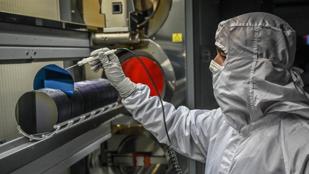
UPVfab, new clean room at UPV
UPVfab Micro-fabrication pilot line
Your partner for backend semiconductor processes.
Researchers from the UPV and joint institutes iTEAM, ITQ, I3M, CI2B and IDM are working on the update, expansión and enhacement of the UPVfab cleanroom, located in the Polytechnic City of Innovation at the Polytechnic University of Valencia. The scientific-technical areas of activity in the room include photonics, electronics and chemistry.
This facility has its origins in the private initiative of the extinct Valencian company Siliken Energy between 2009 and 2012. After a period of inactivity, the company Espectrolítica S.L., with a project for Austria Micro-Systems, brought this cleanroom (500m2, class ISO-7) back into operation. Since 2018 the control is by the UPV, and in 2021 it has received the approval and recognition by the Social Council of the UPV as corporate laboratory.
Since 2018, infrastructure resources has been obtained with public funds, the bulk of which, €3 million, comes from the GVA programmes IDIFEDER/2018/042, IDIFEDER/2020/028 and IDIFEDER/2021/046, and from industry equipment transfers valued at €1.5 million.
UPVfab positions itself as a catalyst for industry through a resident company programme, whose first company is the spin-off VLC Photonics. This programme aims to incorporate a dozen companies in the next three years.
"Such facility makes no sense if, in addition to basic R&D, we don't involve industry, to train the graduates of the future and develop the technological processes that are of interest to it" says Pascual Muñoz, current director of UPVfab.
Even with the global uncertainty in the supply of semiconductor components in particular, and raw materials in general, the UPVfab team has a development and consolidation plan for the facility that includes new equipment, technological processes and the consolidation of the human resources necessary for this. Muñoz sees this facility as a potential generator of new economy, "We will do well if, in addition to attracting more companies, we generate spin-off companies based on UPVfab developments". He also recognises "the role and need for small foundries in expanding sectors such as integrated photonics". In the area of integrated photonics, UPVfab researchers under contract with Huawei Technologies Canada Ltd. have developed micro-chips for LIDAR, the base technology for future autonomous driving. In addition, they participate in the Huawei Joint Research Center on 6G technologies in developing photonics technology for the RF chips of the future.
In the area of electronic engineering, UPVfab is collaborating with AWSensors, one of the first UPV spin-offs, in the development of its new quartz microbalance biosensor technology for the healthcare market. Antonio Arnau, founder of AWSensors, recognises the fundamental value of this infrastructure, finally recognised as a UPV laboratory. "UPVfab is fundamental for the validation and optimisation of our new array biosensors, which will allow AWSensors to enter into precision medicine through the rapid and simple diagnosis of cancer mutations relevant to the personalised treatment of this disease and also its evolution".
In the area of chemical engineering and the decarbonisation of the process industry, the deposition of functional and/or protective thin films is addressed. This make possible to realise custom-made devices with advanced capabilities and functionalities. Such instruments enable the optimisation of industrial processes such as the separation of gases like H2, O2 or CO2, the conversion or storage of energy in fuel cells and electrolysers, or the production of value-added compounds in electrochemical reactors. This is also a key tool for the intensification of processes producing cleaner, safer, more energy-efficient and zero-impact technologies. Many of the processes are carried out in collaboration with leading companies in the energy and chemical sector, indicating the impact and interest of the technology developed.
The knowledge and developments that can be achieved in the facilities are necessary to increase and innovate in existing spin-off companies, as is the case of Kerionics, dedicated to the production of solid state membranes for the separation of components for energy conversion and storage.
From the point of view of materials characterisation, the facilities already have several high-performance equipment, such as an ellipsometer, a Fourier transform IR spectrometer (FTIR) with high resolutions for the fine study of chemical properties of samples from the size of microstructures of 5 microns up to a 6" wafer. In addition to all these tools, a whole series of equipment is available for the design and manufacture of samples by photolithography and sputtering of both planar and tubular samples, which will allow, in addition to exploring new lines in basic R&D, a development for subsequent scaling up at the industrial level.
Proyectos y Servicios IT & IoT
2yFor many people this is science fiction, or even achievements made abroad, showing local successes, is valuing our society. Mr. Pascual congratulations to you and your team.
Free Space Optical Comms (FSOC) and Optical Instrumentation System Engineer, at INDRA
2y👏👏 👏 👏 Congratulations to the Universitat Politècnica de València (UPV) and UPVfab Micro-fabrication pilot line for this innovative project. This is the kind of ideas that Spain needs to transform its economy, to create wealth, to generate highly qualified jobs and to impulse private-public collaboration. I wish you the best for the future.
¿Otra?