Oct 10 2019
Using the single-particle spectroscopy method, scientists at the Tokyo Institute of Technology (Tokyo Tech) examined electroluminescence in light-emitting devices.
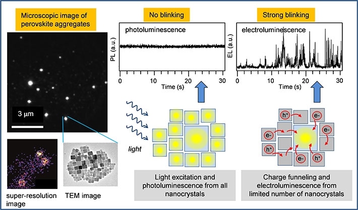 Microscopic emission image of aggregates formed by nanocrystals of the perovskite CsPbBr3 (left, top), and super-resolution analysis of electroluminescence from one such aggregate (left, bottom); Intensity time trace of photoluminescence of one aggregate (middle, top) shows no fluctuations because all nanocrystals within the aggregate emit simultaneously (middle, bottom scheme); Intensity time trace of electroluminescence of one aggregate (right, top) shows strong fluctuations (blinking) because all charges are funneled to one nanocrystal which is emitting (right, bottom scheme). (Image credit: Tokyo Institute of Technology)
They found that the emission blinking phenomenon and efficient charge funneling between single perovskite nanocrystals were responsible for the low efficiencies of perovskite light-emitting devices.
Recently, metal halide perovskites have become a highly promising alternative material for next-generation optoelectronic applications. In particular, nanoscale-sized perovskite structures present striking photophysical properties, like color tunability, direct bandgap, narrow photoluminescence linewidth, and large absorption cross-section.
In addition to their low price, solution processability, possibility for scale-up synthesis, and compatibility with current optoelectronic device components, these properties render metal halide perovskite nanocrystals a useful alternative to other semiconducting materials for wide-ranging light-emitting applications, such as lighting, displays, lasers, and memory devices.
Although perovskite nanocrystals exhibit extremely high photoluminescence yield, electroluminescence devices developed from these nanocrystals have long suffered from low efficiency. While the latest attempts have focused on device design to overcome this issue, thus far, there has been no systematic research on the nanoscale physical origin of the poor efficiencies.
In this study, Prof. Martin Vacha’s group from Tokyo Tech used single-particle microscopic detection and spectroscopy to analyze the electroluminescence phenomenon on the level of single nanocrystals.
The group used nanocrystals of the perovskite CsPbBr3, the surface of which was passivated with oleic acid ligands, dispersed in a thin film of a conducting polymer that was used as an emission layer in a light-emitting device.
The device was created for use over an inverted fluorescence microscope, which allowed comparison of photoluminescence and electroluminescence from the same nanocrystals. The CsPbBr3 nanocrystals develop aggregates in the emission layer, with every aggregate composed of tens to hundreds of single nanocrystals.
Using a state-of-the-art microscopic technique of super-resolution imaging, the scientists discovered that in photoluminescence, all the nanocrystals in the aggregate emit light, whereas in electroluminescence, very few (typically 3–7) nanocrystals actively emit light. The electroluminescence from only a few nanocrystals was due to size distribution and the resultant energy landscape in the aggregate.
Electrical charges introduced into the device at the time of operation are captured on single nanocrystals and are efficiently funneled to the largest nanocrystals. These largest nanocrystals in the aggregate have the least energy bandgap.
Moreover, the conduction and valence bands of the largest nanocrystals function as traps for charges captured initially at the surrounding nanocrystals. The presence of the conductive environment between the nanocrystals facilitates active migration of the charges to these traps from where the electroluminescence occurs.
Another significant outcome is that the electroluminescence intensity from the nanocrystals that actively emit light is not constant. Instead, it exhibits strong fluctuations—the so-called blinking. This blinking is absent in photoluminescence of the same aggregates. The scientists have previously shown that the blinking can be caused by both the externally applied electric field and the conductive matrix (see ACS Nano 13, 2019, 624).
The blinking phenomenon in the light-emitting device is a vital factor that can bring down the efficiency in electroluminescence. The scientists summarized that electroluminescence efficiency is only about one-third of that of photoluminescence because of the existence of the blinking phenomenon.
This study presents a method for efficient nanoscale characterization of electroluminescence of halide perovskite materials for light-emitting applications. One of the solutions with regard to greater efficiency will be surface engineering of the nanocrystals that would overcome the intensity fluctuations.
Source: https://www.titech.ac.jp/english/