August 4, 2016

When it comes to materials science, a better understanding of how heat moves through materials at the atomic level would go a long way toward improving the design process. Scientists already understand the limitations of thermal energy in materials: the second law of thermodynamics dictates that an energy conversion process can’t be entirely efficient. Heat waste will negatively affect or limit some industrial process (such as energy transmission) more than others. For these industries, learning to recycle heat energy into useful work would be a major breakthrough.
As the old saying goes, “If you can’t measure it, you can’t manage it.” Measuring how heat travels, up until now, has been a challenge. While photographing the process could help yield vital insights into how to design better materials, the speeds and scales necessary to capture the atomic oscillations that dictate heat transport -- scale measured in nanometers, and speeds in picoseconds -- hasn’t been possible, even with the most sophisticated electronic triggering schemes.
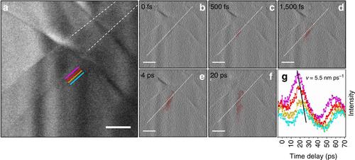
Recently, a team of researchers from the University of Minnesota employed an ultrafast electron microscope to capture and record how heat moves through materials at the nanoscale traveling at the speed of sound.

“Relevant phonon wavelengths for heat transport are typically under 500 nanometers, meaning typical diffraction-limited optical probes have insufficient resolving power,” Dayne Plemmons, a graduate student who co-authored the research paper, told Design News. “Observing coherent phonon transport requires a technique with nanometer spatial resolution, few femtosecond/picosecond temporal resolution, and a contrast mechanism sufficient to distinguish few milliradian angular perturbations in atomic planes,” he said.
The research team achieved the required spatial resolution and contrast using a FEI Tecnai Femto transmission electron microscope [TEM]. With a brief laser pulse, they excited electrons and rapidly heated crystalline semiconducting materials of tungsten diselenide and germanium.
“[The TEM] employs relativistic electrons with ultra-short wavelength to condense the diffraction-limit below an Ångstrom (in reality the resolution is dictated by lens aberrations),” said Plemmons. “The technique, called bright-field imaging, filters out electrons that have been elastically scattered (diffracted by atomic planes) and thus minor perturbations from the Bragg condition result in contrast in the images.”
The result has been photography of a process that has never been captured before. Slow-motion videos (a billion times slower than normal speeds) caught the resulting waves of energy moving through the crystals. Although TEM has existed for decades, the new research has made key advancements in the extension of the analytical capabilities of the TEM to the ultrafast time-scale. This was achieved by operating the TEM stroboscopically, meaning a synchronized pulse-train of probing electrons and timing (or excitation) photon pulses were used to acquire the requisite signal for a single time-point. The researchers say it’s a critical step in understanding how scattering rates and velocities due to imperfections at the atomic level can dictate a material’s thermal conductivity.
“If we consider that a large majority of heat is removed by convective processes (water-chillers, fans) we now have an excess of material with a low amount of heat to extract which, by the second law of thermodynamics, becomes increasingly difficult to extract,” said Plemmons. “In the solid-state, however, we typically think of conductive heat transport. Conduction is described by millions upon millions of largely random scattering of the phonons.”
About the Author(s)
You May Also Like


