The World's Smallest LED: A Novel Approach to Digital Holographic Microscopy
23-05-2023 | By Robin Mitchell
Recently, researchers from multiple institutions around the world have worked together to create the world’s smallest LED that was then used to turn existing CMOS image sensors into holographic microscopes. What challenges does common microscopy face, what did the researchers develop, and how could such technologies change the future?
What challenges does common microscopy face?
The 17th century was arguably one of the most exciting periods of scientific history, thanks to the efforts of many famous scientists, including Isaac Newton, Robert Hook, Robert Boyle, and Johannes Kepler. Whether it was prisms and the nature of light, the forces that govern the universe, or the relationship between planetary bodies, there is no doubt that modern science would not be what it is today thanks to these discoveries and inventions. Of the many inventions during this time period, the microscope was one that helped to launch numerous discoveries in the field of medicine and biology, as this field of study is generally focused on the microscopic world.
But for all the benefits that the development of the microscope has provided, there are numerous challenges that they continue to face. One such challenge is the resolution that they can provide. Simply put, microscopes are dependent on a strong source of light to provide illumination, but as light has a finite wavelength, objects smaller than this wavelength can be difficult (if not impossible) to resolve.
The depth of field offered by microscopes can also be problematic, as the use of powerful lenses can create extremely shallow depths of field, which result in only a very narrow plane being in focus. For example, a spherical object will not appear to be spherical but instead as a flat 2D structure (adjusting the focus will bring different layers of the object into focus).
The need for lenses also introduces challenges, as lenses can be extremely expensive due to the need for high-quality glass that is carefully shaped and treated. This can also have an impact on the overall size of the microscope, with large microscopes being heavy. Large microscopes are also impractical for portable use, which can see researchers required to travel to remote locations to gather samples and return them to laboratory environments.
Sub-Wavelength Si LED in CMOS Platform
In recent years, the integration of photonic components into microelectronics platforms has been a significant advancement in the field. However, the development of a small and bright on-chip light source has remained a challenge. This article discusses a breakthrough in this area with the creation of a nanoscale on-chip light source with high intensity, specifically, an electrically driven Si light-emitting diode (LED) with sub-wavelength emission area fabricated in an open-foundry microelectronics complementary metal-oxide-semiconductor (CMOS) platform.
The LED emission spectrum is centred around 1100 nm, and the emission area is smaller than 0.14 μm2. This LED has a high spatial intensity of >50 mW/cm2, comparable with state-of-the-art Si-based emitters with much larger emission areas. Due to sub-wavelength confinement, the emission exhibits a high degree of spatial coherence, demonstrated by incorporating the LED into a compact lensless in-line holographic microscope. This centimetre-scale, all-silicon microscope utilises a single emitter to simultaneously illuminate ~9.5 million pixels of a CMOS imager.
Researchers develop world’s smallest LED for digital holographic microscopy
Recently, a large team of researchers from the Disruptive & Sustainable Technologies for Agricultural Precision (DiSTAP) and the Critical Analytics for Manufacturing Personalised-Medicine (CAMP) Interdisciplinary Research Groups (IRG) of Singapore-MIT Alliance for Research and Technology (SMART) developed the world’s smallest LED measuring just 400nm in diameter with an area of 0.14µm2 with the goal of creating an LED suitable for low-cost digital holographic microscopy.
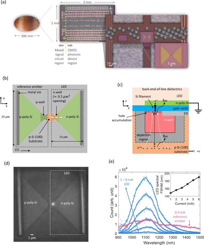 Image (a) displays a fully fabricated 300 mm wafer with integrated monolithic electronics and photonics alongside a detailed optical micrograph of a diced, unpackaged chip with various active and passive photonic components and mixed-signal circuits. Close-ups of the LED and the reference emitter on this chip are also featured. A schematic top view (b) of the LED and the reference emitter omits the back-end-of-line (BEOL) dielectrics and the gate oxide but highlights the shallow trench insulator (STI). A zoomed-in side view (c) along a white dashed line reveals the LED and corresponding carrier transport, with solid and hollow circles indicating electrons and holes, respectively. The LED, when biased at 6 mA, is shown in a micrograph (d), with wide-field illumination light from a commercial LED centred around 1100 nm. Finally, the spectra of the LED and the reference emitter (e) were measured by routing the emission through a single-mode fiber into a spectrometer, with raw data represented by hollow circles and Savitzky-Golay filter results by solid lines. The spectral full-width-half-maximum (FWHM) of the LED is presented in the inset.
The significance of the new LED is twofold; the first is that the LED is smaller than the wavelength of light that it produces, far infrared with a wavelength of 1100nm. The second is that the researchers were able to develop the LED using Silicon as the optical component as opposed to more exotic materials generally used in LEDs (such as gallium and germanium). Thus the new LED can be manufactured using standard CMOS foundry practices. For the LED to work, the researchers needed to create a Si filament that provides a highly conductive channel, and this was achieved by electrically stressing a layer of SiO. The breakdown of this layer using a large voltage and current breaks the SiO bond, leaving behind a thin filament of Si. Simply put, this technique is not entirely dissimilar to the first point-contact transistors, where customers had to “burn” the parts in before they could be used.
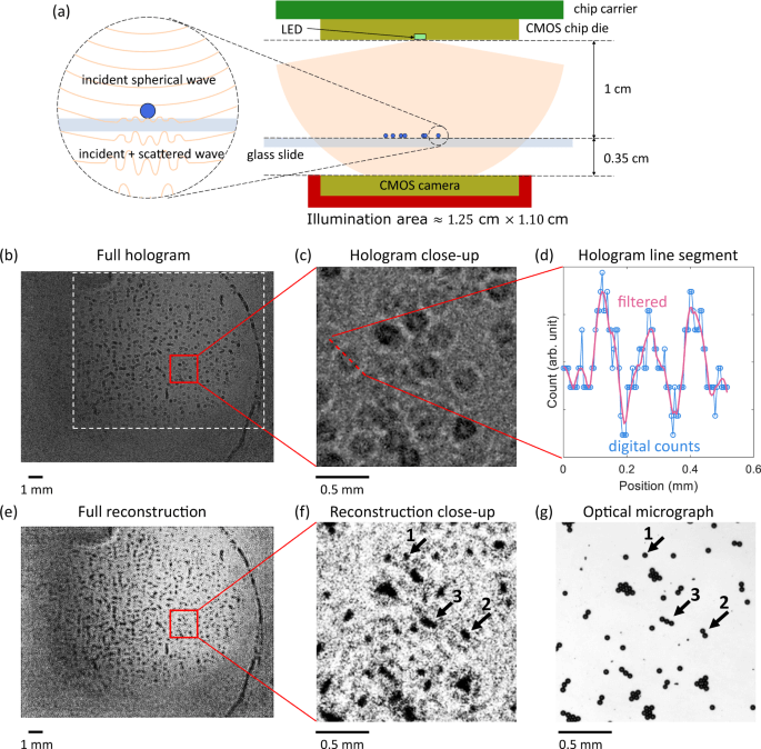
However, the purpose of the new LED wasn’t to create the world’s smallest LED but to help enable digital holographic microscopy using regular CMOS image sensors. The small size and high intensity of the LED creates a beam of infrared light with a wide angle, and this circular emission of light is then passed through a glass slide with a sample. Instead of creating a shadow, the light interacts with the sample and produces an incident + scattered wavefront that is then casted onto a CMOS sensor.
To further understand the significance of this development, it's worth delving into the specifics of the research that led to the creation of this LED. In a groundbreaking study published in Nature Communications, researchers have reported the development of an electrically driven silicon (Si) light-emitting diode (LED) with a sub-wavelength emission area. This LED was fabricated in an open-foundry microelectronics complementary metal-oxide-semiconductor (CMOS) platform, a standard integrated circuit technology. The emission spectrum of the LED is centred around 1100 nm, and the emission area is smaller than 0.14 μm², which is approximately 400 nm in diameter.
This LED exhibits a high spatial intensity of over 50 mW/cm², a value that is comparable with state-of-the-art Si-based emitters with much larger emission areas. The LED's emission exhibits a high degree of spatial coherence due to sub-wavelength confinement. This feature was demonstrated by incorporating the LED into a compact lensless in-line holographic microscope. This centimetre-scale, all-silicon microscope uses a single emitter to simultaneously illuminate approximately 9.5 million pixels of a CMOS imager.
The development of this nanoscale on-chip light source is a significant step forward for integrated photonics systems. It addresses the challenge of creating a small and bright on-chip emitter, which has been a limiting factor in the scalability of photonic chips. This advancement could have far-reaching implications for various applications, including data communication, sensing, imaging, and quantum computing.
The image series (a-c) presents the emission pattern at multiple currents with 50 ms integration, captured using a microscope equipped with a 100×, 0.95NA objective and an InGaAs camera. The chip die was wirebonded to a chip carrier, which was fixed on a piezo translation stage. A 2D Gaussian fit of the emission pattern at 6 mA is shown (d). The n+/n emission power and the associated external quantum efficiency (EQE), neglecting the background emission, are displayed (e). The inset shows the forward bias voltage versus current. Cross-sections of the fit emission pattern at 6 mA from -5 to 5 μm are shown in both x and y axes (f, g). The deconvolved emission area and spatial intensity are presented (h), based on the spatial full-width-half-maximum (FWHM) of the point-spread function (PSF) of the microscope. The single-mode fiber (SMF) coupled power and coupling efficiency are also shown. The error bars in various figures represent the 95% confidence interval of the corresponding fitting parameters or the error propagation considering the PSF measurement error and the fit error in e.
With the use of specially developed AI tools, the resulting sensor data can be used to generate an image of the sample. The demonstration done by the researchers is significant as not only does the AI require no initial training (whereas other models typically do), but off-the-shelf CMOS technologies can be used to generate images, including those found in smartphones.
How could such technologies change the future?
The researchers hope that future versions of smartphone cameras will be able to integrate such technologies for the purpose of remote microscopy (i.e., away from the lab). One such industry that could massively benefit from digital holographic microscopy is agriculture, where site workers can use a smartphone to observe living cell samples in plants to provide better diagnoses of their health.
The development of the miniature LED could also lead to miniaturised optical communication between different chips, thereby eliminating the need for bulky photodevices and cumbersome fibre optic cables. This could even allow for communication inside a single chip, using high-intensity IR LEDs to transmit data from one side of a chip to the other. It is also believed that the LED could be scaled up to provide significant IR output, something which could benefit night vision and other IR technologies.
What the researchers have developed is truly exciting, and the combination of miniature IR sources along with AI and CMOS image sensors could bring a whole new range of features to the next generation of smartphones.
