A few years ago there was a rash of research papers describing the use of biological techniques to manipulate matter on a molecule-by-molecule or particle-by-particle basis.
The spread of powerful analysis tools, imaging techniques and massively parallel synthetic chemistry combined to kick-start these attempts to harness nature’s so-called bottom-up approach to construction.
Breakthrough publications covered, among other things, building transistors by using DNA to guide carbon nanotubes into specific sites, and breeding mis-folded proteins so that gold atoms stuck to them and formed nanowires.
Since then progress has been steady, but unspectacular, with not much to report in the way of systems with any commercial relevance. However, the idea behind pursuing biological processes is that they can do things we so far have not been able to – like fashion nanoscale patterns at room temperature and pressure, without aggressive chemicals or big, expensive lithography machines.
“When you look at the way nature manufactures things using proteins, things like bone, seashells and so on, what you’ll observe is a very sophisticated technology for manufacturing things from solution phase in a bottom up fashion,” says Hash Pakbaz, v-p of business development at US start-up Cambrios Technologies.
 |
|
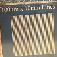
A thin-film created by Cambrios |
Cambrios uses massively parallel screening techniques to find peptides, the short chain molecules that go to make up proteins, that selectively bind particles of semiconductor and metal. It can then take advantage of the self-aligning properties of the peptides to create high-quality layers of the semiconductor on a substrate.
The selectivity of the organic molecules is so high that the deposited layer consists uniformly of a single crystal structure, something which enhances its electronic properties.
However, while eventually Pakbaz expects the techniques Cambrios is developing to enable the construction of functional devices, in the short term the company is focusing on using biology to make an impact on the existing semiconductor and display manufacturing flows.
“Our aim is to introduce materials that people can use in existing manufacturing facilities, and use those materials to deposit thin films of materials that they cannot currently deposit, or that cannot be deposited cost effectively,” says Pakbaz. “Or they might not be able to get the performance they need because particular processes lead to amorphous films, whereas we think we have a lot of control over material structure from the bottom up, to be able to create materials that are polycrystalline.”
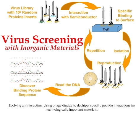 |
| This process is used by Cambrios to discover specific proteins that bind to the desired electronic materials. |
Other biology-inspired research looks to be moving more slowly. For example, using long chains of amyloid fibres – the stuff associated with degenerative brain disease such as Alzheimer’s – as templates for tiny wires. This was originally shown two years ago, but there has been slow progress towards making meaningful use of the approach.
“The use of self-assembling peptide fibres can be technically quite difficult, so I think it’s a slow-moving process, but it is still progressing. Like all research it proceeds slowly,” says Dr Glyn Devlin, who is investigating amyloids at the University of Cambridge. “Having an understanding of how they form is a key to using them as a nano scaffold.”
One company that is already employing biology to improve on existing technology is Bristol-based Nanomagnetics, which uses the protein ferritin to act as a template for controlling the orientation and size of magnetic grains to make hard disk recording media. The technique ensures the particles are of uniform size, evenly spaced and insulated from one another in a carbon matrix.
Storage density of products made using the company’s Dataink material could be very high. It has said that a floppy disk-style 1.8in. drive could store 4.7Gbyte of data, the same as a DVD.
However, both Nanomagnetics and Cambrios Technologies are in a minority. Most work to develop and control some aspect of biology in order to be able to manipulate matter on the nanoscale is going on in academic labs. It is very early days for the whole field, and these are its first faltering steps.
Dr Wilhelm Huck, a researcher in the Department of Chemistry at Cambridge, thinks there are some fairly basic problems that still need to be overcome with a lot of the work. Huck works with polymers, trying to get them to self-organise into ordered shapes, and says he is having considerable success working on length scales of 5-100nm. Molecular electronics, on the other hand, is a different kettle of fish.
“I think the field is going in two directions,” says Huck. “You have the people doing molecular electronics and I think they are still a little bit stuck. You can fairly easily organise your molecules – you just need one or two or three and they will be the actual device. But it’s not quite understood how a molecular device actually works, and how to link up to a molecular device.”
So how do you have your electrodes connecting?
Although the electronic properties of polymers are often not quite good enough to make really effective devices, certainly well-below what might be achievable with a crystalline material, they can apparently be manipulated with very good control.
“It’s not so difficult at all to make feature sizes either by using top down or by using self organisation in the 100nm or smaller size regime,” says Huck. “I think the aim there, and it’s going extremely well at the moment, is to use extra organisation at the 10-100nm level and you should be able to make your polymeric materials behave a bit more like small molecule crystals. You increase the ordering and that greatly increases the functionality as well.”
It looks like it will be a while before either biologically inspired processes or devices actually made from biological units really make in-roads into current electronics. But who knows, we might one day look back on this pioneering work and see that it marked the birth of a whole new era.
www.cambrios.com
www.cure.group.cam.ac.uk
www-huckgroup.ch.cam.ac.uk