Single-wire data transmission is useful when operating a multitude of disperse components if high speed isn’t a requirement, but there’s a need for flexibility. The approach reduces the number of conductors in the cabling by shrinking size and cost. It can also improve system reliability.
Dialog Semiconductor’s GreenPAK is a lower-power, NVM-programmable FPGA that’s used in this article to implement serial-to-parallel converters using a single-wire line.
Main Idea Behind the Method
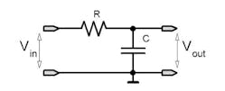
Let’s start with the classic integrating RC element (Fig. 1) and its properties. The integrating RC element can be used in logical and digital circuits to change the pulse length or, more precisely, generate or extend the pulse duration, process the pulses using the integral law, etc.
As is known, the capacitor voltage can’t be changed instantly. Its charge and discharge time depend on the capacity of capacitor C and the resistance of resistor R. This time can be evaluated using the time constant of the RC element calculated according to the formula: τ = RC.
If a sufficiently long pulse is sent to the input of the integrating element, the capacitor will have time to fully charge and discharge. But if the pulse is short, much shorter than the time constant τ, then the capacitor C voltage will hardly change.
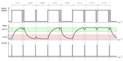
To transmit the serial code, we need to have two data lines—Data and Clock. If Data is being transmitted with broad pulses that have time to recharge the capacitor of the RC element, and Clock is being transmitted with narrow, short pulses that can’t pass through the integrating element, then it’s possible to combine these two lines into one. Thus, the integrating RC element will serve as a separator for the signal receiver (Fig. 2).
It’s necessary to take the Clock signal before the RC element, with only the rising edge being important, and the Data signal after the RC element. Then, if you correctly generate the transmission signal of bit sequence, the problem is solved. Figure 2 shows an example of a byte 10010111 (input signal) generated for transmission.
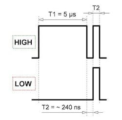
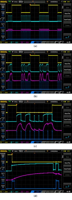
One can readily see that in order to transmit logical data “one/zero,” it’s necessary to generate a corresponding “high/low” sufficiently wide pulse with a short Clock pulse at the end (Fig. 3).
At this point, a careful reader may ask a logical question: Why use an external RC element to separate the Data and Clock signals when this can be done directly using the classical delay element? Looking ahead, we can say that the use of an external RC element allowed us to significantly reduce the current consumed by the receiver, because we stopped using an internal oscillator required for the delay element to operate.
The Data signal voltage received after passing the RC element must be within a certain range of logic one voltage (green area of Fig. 2). The Clock signal voltage should not pass through the RC element and not extend beyond the range of logic zero voltage (red area of Fig. 2). There’s an ambiguity area between them, where the existence of erroneous states is entirely possible. Therefore, the capacitor’s capacity and resistor’s resistance must be selected so that all “charge/discharge” transient voltage values don’t fall into this area. Here’s how this is done:
Let’s consider the integrating RC element from Figure 1 as a series connection of resistor R and capacitor C. The following formula is used for such a circuit:
Given that:
we can write the following differential equation with respect to the capacitor voltage, which, in fact, is the output voltage of our integrating element VC = Vout:
The solution of this differential equation is well known:
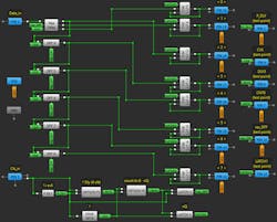
After the signals are separated by an external RC element (Fig. 14) the Data signal coming from the input PIN#2 (Fig. 9) is fed into the first trigger of the trigger chain. Then, we select only the rising edge of the Clock signal PIN#5 using the P DLY detector and form a clock signal for the trigger chain and counter CNT2. When the internal CNT2 signal is low (Fig. 9, CNT2 signal), the serial code is decoded into the parallel code on the trigger chain, where triggers are in operation due to the high resDFF signal coming from the output of the FILTER0 inverter.
The signal indicating the current state of each trigger is fed into the respective latch and stored when the CNT2 signal changes from low to high. At the same time, the triggers of the decoding chain are reset to the initial state, as the resDFF signal changes from high to low. The latch stored signal is fed into the corresponding output PIN during the time when the “CNT2” signal is high—this time, in turn, it corresponds to the time t2 between the generated data packets in the Transmitter_170 design.
The DFF5 trigger doesn’t have an nRESET output. Therefore, it has an additional reset logic circuit based on 4-bit LUT0 and 2-bit LUT1 elements as described in AN-1029.
Looking carefully at the initial conditions for launching the Transmitter_170 and Receiver_170 designs, one drawback is noticeable. If the receiver starts its operation later than the transmitter, then the conversion of serial code to parallel may not start from the beginning of the data packet, but from, say, the middle. This, in turn, will cause a shift in the data-output process. Thus, to ensure correct operation of the transmitter-receiver, it’s necessary for the receiver to start operating simultaneously with the transmitter; in other words, they must have a common power source (Fig. 14, below).
One way to eliminate this drawback is, for example, to transmit a service auxiliary signal at the beginning of each data packet to reset all triggers in the receiver design before starting the process of converting serial data. It will ensure that the process of data conversion starts at the beginning of the package. This way we will get a reliable data-transmission system, where the transmitter and receiver can have their own power sources and start operating at any time, independently of each other. To test this, another pair of Transmitter_533 and Receiver_533 was created (Fig. 15, further below).
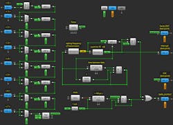
The design of Transmitter_533 (Fig. 10) also consists of two main components:
- Parallel-to-serial converter based on 2-bit LUT3, 3-bit LUT14 ÷ 3-bit LUT17, 3-bit LUT5 ÷ 3-bit LUT7, DFF2, DFF0, DFF5 ÷ DFF9, and Pipe Delay
- Generator generating the necessary bit sequence transmission signal based on CNT5, CNT6, DLY0, DLY1, DFF4, 3-bit LUT0, 3-bit LUT13, EDGE DET0, P DLY, 4-bit LUT2, and 2-bit LUT1
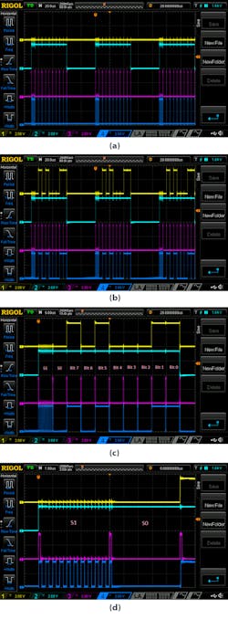
The operational principle of this design is no different from the previous one. Similarly, the CNT5 counter defines the transmission signal time of 5 µs. However, unlike the previous design, the CNT6 counter forms a packet of 10 such time periods. That is, apart from eight periods designed to transmit data, two additional time periods—S1, S0—are used to generate the required service signals (Fig. 11c).
There may be many ways to create a special service signal and then detect it in the receiver. We chose the first one that came to mind: Using DFF4 and 3-bit LUT0, the S1 time period of the service signal is filled with an oscillator frequency of 2 MHz and mixed with the main transmission signal using 2-bit LUT1. The S0 period is left without any changes (Fig. 11d). The reasons for this will be explained in the description of the receiver design.
Like in the previous transmitter design, the delay element DLY0 together with the 3-bit LUT13 elements and the falling edge detector EDGE DET0 make it possible to change the time duration between the generated data packets. The desired specific form of the output signal (Fig. 3) is created just as in the previous case—based on DLY1, 4-bit LUT2, and P DLY. Since the data package consists of 10 time periods, it’s necessary to add two triggers to the chain to correctly generate the serial code. This is done on Pipe Delay, where OUT0 is set at = 3.
Therefore, besides the data byte, two additional bits—S1 and S0—are transmitted in the design of Transmitter_533. The S1 bit is filled with a periodic signal with an oscillator frequency of 2 MHz.
The design of Receiver_533 (Fig. 12), like the previous one, performs the inverse function of decoding the serial code into the parallel one. In addition, it detects the service signal (generated by the transmitter) and resets all triggers before starting the process of converting serial data.
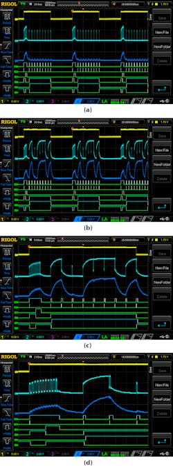
This function is performed using the DLY5 delay element, where PIN #5 serves as a clock signal source; i.e., the Clock signal before the RC element. The response of the detector P DLY of both edges to the periodic signal, at a 2-MHz frequency filling the additional S1 bit, will be similar to the filter response, which means it’s possible to generate a launch signal for DLY5 (Figure 13, P_DLY signal).
DLY5 is a delay element on the rising edge, which is why one can readily see that DLY5 will work only when the additional S1 bit arrives (Fig. 13, DLY5 signal). In its turn, the DLY5 delay element will always generate a reset signal for the CNT6 counter before starting parallel-to-serial conversion. In this way, the CNT6 counter and two latches—LATCH1 and LATCH2—will generate the necessary signals to reset triggers (Figure 13, res_DFF signal) in the decoding chain. In addition, the signal for latching data in the output latches 3-bit LUT5, 3-bit LUT6, and 3-bit LUT12 ÷ 3-bit LUT16 during the parallel data output (Fig. 13, LATCH1 signal).
The signal, with its 2-MHz frequency filling the additional S1 bit, meets the requirement for not passing the RC element. However, due to its multiple repetitions during 5 µs, the duration of one bit was chosen, and thus it manages to charge the capacitor to a voltage level that can be identified as a logical one. Subsequently, to allow the capacitor to discharge to a guaranteed logic zero level and not be able to affect Bit 7 of the data signal, we use the second additional S0 bit.
Furthermore, to improve the system’s reliability, the clock signal for the trigger chain and counter CNT6 is formed by the rising edge detector EDGE DET0, where the signal is taken after the P DLY element. This, in turn, will prevent a parasitic clock signal CLK from being generated during decoding of service S1 bit (Fig. 13, “CLK” signal).
The rest of the elements perform the same functions as in the previous design.
Circuit Analysis
As already mentioned, to demonstrate the efficiency of the presented data transmission principle, we created a pair of transmitter-receiver devices.
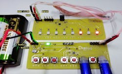
As noted above, the Transmitter_170 – Receiver_170 pair (Fig. 14) has a common power supply determined by the used 78L33 line stabilizer, and it’s 3.3 V. There are eight buttons S0 ÷ S7 employed in the transmitter circuit to generate the desired transmission signal. Accordingly, the eight LED0 ÷ LED7 LEDs in the receiver circuit serve to visualize the received and decoded signal.
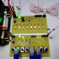
The transmitter and receiver in the Transmitter_533 – Receiver_533 pair (Fig. 15) have independent power supply nodes and, as described above, represent an independent data reception-transmission system. Like the previous circuit, the buttons S0 ÷ S7 can be used to set the desired transmission signal; the result can be monitored by the LED0 ÷ LED7 LEDs in the receiver circuit.
We’ve measured the current consumed by chips during the operation of the presented pairs of transmitter-receiver—IC1 circuit of Receiver_170 and IC2 circuit of Receiver_533—together with their R1C1 elements, without considering the current consumed by LEDs. As it turned out, the measured current values also depend on the number of logical ones transmitted in the byte of the serial signal (this is due to the charge current of the capacitor of RC element). For comparison, the measurement results are summarized in Figure 16.
The measured current values indicate that the current consumed by the chip of the Receiver_533 circuit is slightly higher than the current of the Receiver_170 circuit. That’s because the transmission signal in the Receiver_533 circuit is longer by two bits due to the use of additional auxiliary service bits S1 and S0. Therefore, it can be summed up that the current consumed by the chip with RC element is much less than the current consumed by the chip with the OSC 2-MHz oscillator on.
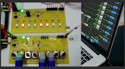
Figures 17 and 18 demonstrate the operating data transmission-reception system based on the operational principle presented above.
Conclusions
The proposed alternative method of transmitting serial data over a single-wire line is quite efficient and competitive—except, of course, in the cases of complex and specific electronic systems. This is fully confirmed by two data transmission-reception systems based on this principle and comprehensive tests of their operation.
Oleksiy Kravchenko is an Applications Engineer at Dialog Semiconductor based in Lviv, Ukraine.
References
GreenPAK Designer Software, Software Download and User Guide, Dialog Semiconductor
GreenPAK Development Tools, GreenPAK Development Tools Webpage, Dialog Semiconductor
GreenPAK Application Notes, GreenPAK Application Notes Webpage, Dialog Semiconductor
AN-1028 GPIO ExpanderSingle Wire Interface, Application Note, Dialog Semiconductor
AN-1029 Adding nSETnRESET to DFF's, Application Note, Dialog Semiconductor
