

What do you think about when you hear the phrase “printed electronics”? To be honest, if you’d asked me yesterday, I would have probably waffled on about using printing techniques to implement components like capacitors, resistors, and inductors on hybrid substrates, multi-chip-modules (MCMs), and some specialized forms of printed circuit boards (PCBs), but I was just talking with Dr. Florian Ullrich from InnovationLab, and he has opened my eyes to a whole new world of organic printed electronics possibilities and potentialities.
As an aside, speaking of waffling, would you believe that even though I’ve now lived in the USA for 31 years as I pen these words, I have yet to sample that pinnacle of American cuisine – the waffle. As you doubtless know, the origin of this delectable dish dates back to ancient times when the Greeks started cooking flat cakes, called obelios, between hot metal plates. Early incarnations were comprised of only flour and water, but they evolved over time. As this form of fodder spread throughout northwestern continental Europe, adopting the name oublies on the way, additional ingredients – including cream and eggs – were added to the mix. Eventually, these little scamps became so popular that the oublieurs guild was formed in 1270.
The art of waffle-making eventually made its way to the New World with Dutch colonists in the 1620s. The word “waffle” itself first appears in the English language in 1725, derived from the Dutch wafel, which itself derives from the Middle Dutch wafele. The earliest waffle irons originated in the Netherlands circa the 14th century. These consisted of two hinged iron plates connected to two long wooden handles that were held over a hearth fire for baking (the plates were held over the fire, not the handles, unless the chef was a devotee of experimental cuisine). Unlike modern minimalist manifestations, the plates at that time were often imprinted with elaborate patterns, such as coats of arms, landscapes, religious symbols, and so forth.
In 1869, the American Inventor Cornelius Swartwout – a name that (unlike a waffle drenched in syrup) rolls off the tongue – was awarded US patent 94043A for an “Improvement in Waffle-Irons,” consisting of a novel handle for opening, closing, and turning a stovetop waffle iron.
Now that I’ve commenced waffling about waffles, I’m finding it difficult to cease. For example, although “waffle” as a noun refers to a baked batter-cake consumable, “waffle” as a verb traditionally means “to use a lot of words without saying anything of importance or interest.” Of course, when I waffle, I engage in the other kind – the type that is replete with nuggets of knowledge and tidbits of trivia, as I’m sure you will agree.
Speaking of which, I now feel moved to have a little waffle about PCBs. I don’t know about you, but modern PCB technologies – with multiple power, ground, and signal layers coupled with tracks that are only a few thousands of an inch wide – blow me away. When I was a young lad circa the 1970s, most of the PCBs with which I came into contact were single- or double-sided with tracks that were 1/8 of an inch wide or more (at least, that’s the way they appear in what I laughingly call my memory).
I remember when I was around 10 years old opening an old vacuum-tube-based television set to gaze in awe at its main circuit board, which was formed from an insulating sheet with holes drilled through it. The component leads (or socket pins, in the case of the tubes) were pushed through the holes, and wires were hand-soldered on the underside. Now that I come to think about it, I also remember my mother’s high-pitched shrieking when she eventually stuck her nose into our family room to see why I was being so quiet. Do you remember the cartoon in which Young Dilbert’s mother is informed that he has The Knack? Well, I think the creators of that sketch got the idea by reading my own mother’s diary.
Returning to circuit boards, another approach of interest, one that predates your humble narrator, was known as cordwood construction in which axial-leaded components were mounted between two parallel plates. The plates themselves were formed from an insulating material, while the component leads were connected together with jumper wires.
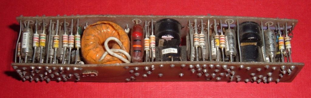
A cordwood module (Image source: Arnold Reinhold/Wikipedia)
Although cordwood construction may seem frightfully “clunky” now, it was the bee’s knees in its day for applications in which space was at a premium (e.g., missile guidance systems) or where minimizing the lengths of traces was important (e.g., high-speed computers).
As another aside, in addition to being a colloquial expression for something or someone excellent, surpassingly wonderful, or cool (synonyms include “the cat’s meow,” “the cat’s pajamas,” and “the bomb”), the “bee’s knees,” meaning “the best,” is also the name of a Prohibition Era cocktail made with gin, fresh lemon juice, and honey, served shaken and chilled, often with a lemon twist or a sprig of basil as a garnish. Hmmm, now I’m feeling thirsty. Anyone for cocktails? But we digress…
The PCBs we know and love today really started to take off in the 1960s, but when do you think this technology originated? In fact, circuit boards have a long and storied history. As I wrote in Bebop to the Boolean Boogie (An Unconventional Guide to Electronics):
The great American inventor Thomas Alva Edison had some ideas about connecting electronic circuits together. In a note to Frank Sprague, founder of Sprague Electric, Edison outlined several concepts for printing additive traces on an insulating base. He even talked about the possibility of using conductive inks (it was many decades before this technology came to fruition).
In 1903, Albert Hanson (a Berliner living in London) obtained a British patent for a number of processes for forming electrical conductors on an insulating base material. One of these described a technique for cutting or stamping traces out of copper foil and then sticking them to the base. Hanson also came up with the idea of double-sided boards and through-holes (which were selectively connected by wires).
In 1913, Arthur Berry filed a British patent for covering a substrate with a layer of copper and selectively etching parts of it away to leave tracks. In another British patent issued in 1925, Charles Ducas described etching, plating up, and even multi-layer circuit boards (including the means of interconnecting the layers). For the next few decades, however, it was easier and cheaper to wire boards manually. The real push into circuit boards only came with the invention of the transistor and later the integrated circuit.
By the 1950s, the interconnection technology now known as Printed Wire Boards (PWBs) or Printed Circuit Boards (PCBs) had gained commercial acceptance. Both terms are synonymous, but the former is more commonly used in America, while the latter is predominantly used in Europe and Asia. These circuit boards are often referred to as laminates because they are constructed from thin layers or sheets. In the case of the simpler boards, an insulating base layer has conducting tracks formed on one or both sides. The base layer may technically be referred to as the substrate, but this term is rarely used in the circuit board world.
The original board material was Bakelite, but modern boards are predominantly made from woven glass fibers that are bonded together with an epoxy. The board is cured using a combination of temperature and pressure, which causes the glass fibers to melt and bond together, thereby giving the board strength and rigidity. These materials may also be referred to as organic substrates because epoxies are based on carbon compounds, as are living creatures. The most commonly used board material of this type is known as FR4, where the first two characters stand for “flame retardant,” and you can count the number of people who know what the “4” stands for on the fingers of one hand.
I’m sorry. I know I’ve waffled more than is seemly in polite society, but I find all of this stuff – where technologies came from and why things are the way they are – to be incredibly interesting. And, of course, speaking of interesting, we find ourselves back with those clever guys and gals at InnovationLab and their state-of-the-art printed electronics that support a wide range of novel applications with dramatically reduced costs.
InnovationLab is a one-stop-shop for everything to do with organic printed electronics: they develop and commercialize functional print products; they provide R&D, pilot production, and mass production as services; and they span the gamut from research to industry. In addition to their own in-house expertise and manufacturing capabilities, the folks at InnovationLab team with BASF for materials science; SAP for software integration, the Internet-of-Things (IoT), and artificial intelligence (AI); and Heidelberger (a world leader in printing and in the design, manufacturing, and marketing of commercial printing presses) for high volume production. InnovationLab is also tightly integrated with academia, including the Karlsruhe Institute of Technology and Heidelberg University.
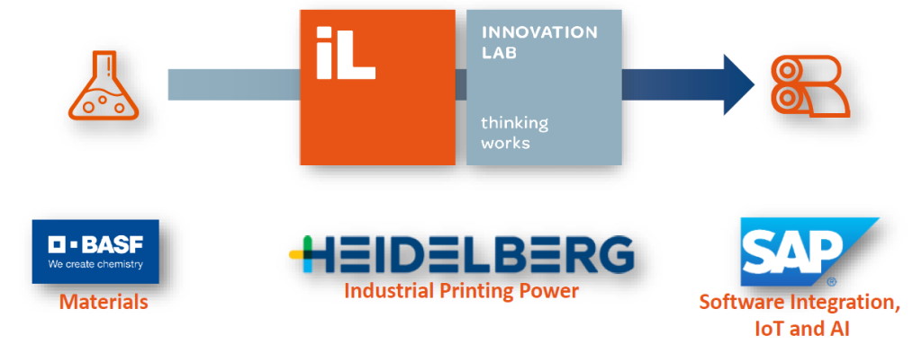
InnovationLab is part of a crack team from academia and industry
(Image source: InnovationLab)
When you hear the term “printed electronics,” you might be tempted to visualize a small-scale operation with people leisurely ambling around screen-printing handcrafted designs onto artisanal substrates. Well, you’d be way off-base in the case of the chaps and chapesses at InnovationLab, whose expertise is in R&D coupled with the enterprise-level production of all forms of printed and organic electronics with a focus on flexible printed pressure sensors.
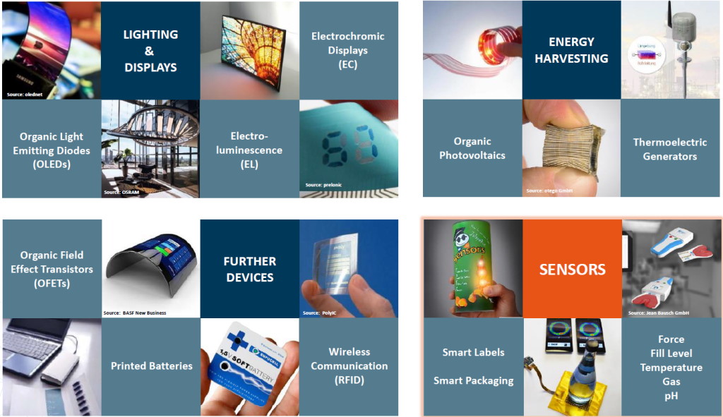
Applications for organic printed electronics (Image source: InnovationLab)
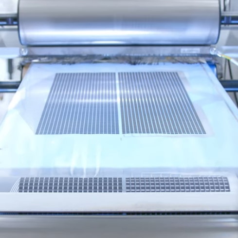
As part of its R&D capability, InnovationLab boasts its own cleanroom and production facility suitable for prototyping projects and small to medium production runs. For larger production tasks – say creating a football field-sized ground-mounted solar panel or pressure-sensing matrix – they turn to the nearby Heidelberger facility, which has machines capable of generating a 33-centimeter-wide strip of printed electronics the height of mount Everest in just one hour. (Not that it’s important, but it tickles my fancy to note that although InnovationLab is located in Heidelburg, the Heidelberger production facility is to be found 12 kilometers away in Wiesloch.)
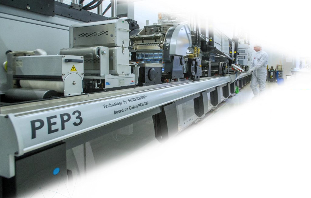
Not your grandmother’s printed electronics printing presses
(Image source: InnovationLab)
So, what sorts of applications can be targeted by organic printed electronics? To be honest, it might be easier to write a list of applications that can’t be targeted, because they pop up all over the place. As an example of a smaller implementation, consider the OccluSense handheld battery-powered device that uses Wi-Fi to transfer data to a corresponding iPad app. The electronic pressure sensors used by OccluSense, which were developed by InnovationLab, allow the detection and recording of masticatory forces in 256 pressure levels. The thin and flexible printed sensor material facilitates the detection and analysis of both static and dynamic forces, while the low cost and material composition allows for single-use sensors that can be discarded in an environmentally safe fashion.
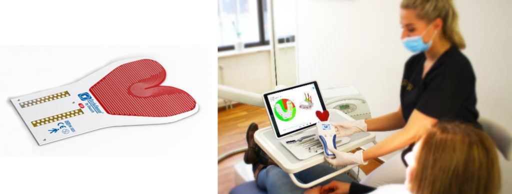
The OccluSense device and advanced printed pressure sensors
(Image source: InnovationLab)
As a slightly larger example – one that is particularly appropriate in this pandemic period — there are smart printed sensor mats that can be deployed at the entrances and exits of stores to allow for automated and anonymous real-time counting of the number of customers inside. This one was of particular interest to me, because – when the COVID-19 pandemic was at its peak – our local Publix store had “Enter Arrow” and “Don’t Enter Cross” patches stuck on the floor at the opposite ends of alternating aisles, if you see what I mean.
The idea was that you had to walk “north” on one aisle and then “south” on the next aisle and so forth. On the one hand, this makes perfect sense. On the other hand, it was a pain in the nether regions if the item you desired was a few feet in on an aisle but you found yourself at the “Don’t Enter” end, which meant you were obliged to trek up one of the adjacent aisles to approach things from another direction. It was particularly galling if the aisle in question was unoccupied at the time.
Now imagine if the entire floor surface of a store were to be covered in a smart sensor and display matrix that started off with “Welcome” arrows presented at both ends of an unoccupied aisle. When a customer entered one end of that aisle, the other end could swap over to display a “No Entry” symbol. This particular example isn’t something that the folks at InnovationLab have actually done – and there would be a lot of “kinks” to work out – but it might be something to consider for the future.
There are so many other possibilities, some of which are presented in a selection of start-ups and spin-offs that have used or are currently using the Start-Up Ecosystem offered by InnovationLab. Also of interest are some recent press releases, such as the one about the smart sensor-infused printed mattress cover for preventing pressure sores on bedridden patients in hospitals and care facilities.
Florian tells me that I have an open invitation to visit InnovationLab if I ever happen to find myself in Heidelberg. I would love to peruse and ponder all of the cool things they are creating with my own eyes, while offering improbable suggestions that would doubtless cause them to roll their eyes. I don’t have any travel plans at the moment, but experience has shown me that you never know what is hiding just over the horizon, so I may well pop up in Heidelberg when Florian and friends least expect it (be afraid, be very afraid). In the meantime, I’d be interested to hear your ideas on any innovative products you think could be created using organic printed electronics.


