About a dozen years ago, I wrote a report on the future of nanomaterials in printing and packaging. I think copies of it may exist today only on my bookshelf, but it has served over that time to inform my opinion on how nanomaterials can be applied to these areas—most recently contributing to piece on these pages a few years back. The basic question: How do you get a nanomaterial onto some packaging cheaply enough that it makes sense for what is essentially a throwaway item?
It has not been easy. But MIT researchers believe they have hit upon a low-cost, robust stamping method that manages to get carbon nanotubes onto a flexible surface so that they can serve as a transistor for controlling individual pixels in high-resolution displays.
In research described in the journal Science Advances, the technique developed for getting the carbon nanotubes onto the surface eschews the use of inkjet printing techniques, which have been thought to be way forward in this application space. Instead they turned to a rather old printing technique: the stamp.
Of course, stamping techniques have been tried before, but they often ran into the same problem as inkjet printing: fuzzy details, with the ink leaving behind coffee ring patterns that compromised the transistor.
“There are critical limitations to existing printing processes in the control they have over the feature size and thickness of the layer that's printed,” said A. John Hart, the MIT associate professor who led the research, in a press release. “For something like a transistor or thin film with particular electrical or optical properties, those characteristics are very important.”
The team’s solution involved using a stamp with a nanoporous surface, meaning it is covered with nanoscale holes. The basic idea was that the ink would be able to pass through the nanopores uniformly and reach the target surface. They looked into the catalogue of nanomaterials and decided upon good old carbon nanotubes—a forest of them.
“It's somewhat serendipitous that the solution to high-resolution printing of electronics leverages our background in making carbon nanotubes for many years,” says Hart. “The forests of carbon nanotubes can transfer ink onto a surface like massive numbers of tiny pen quills.”
To fabricate the nanoporous stamps, the researchers used a technique they had developed previously. They grew the carbon nanotubes into patterns on the surface of silicon. They then coated the nanotubes with polymer that enabled the ink to flow evenly through the forest of nanotubes, and also ensured that the tubes would not become compressed from the stamping action.
While the nanoporous surface was the big breakthrough for this approach, the researchers soon discovered that the success of the technique depended largely on how evenly pressure was applied to the stamp. To determine how to best apply the pressure, the researchers also developed a predictive computer model that calculated the amount of force necessary to leave behind an even layer of ink on the target surface.
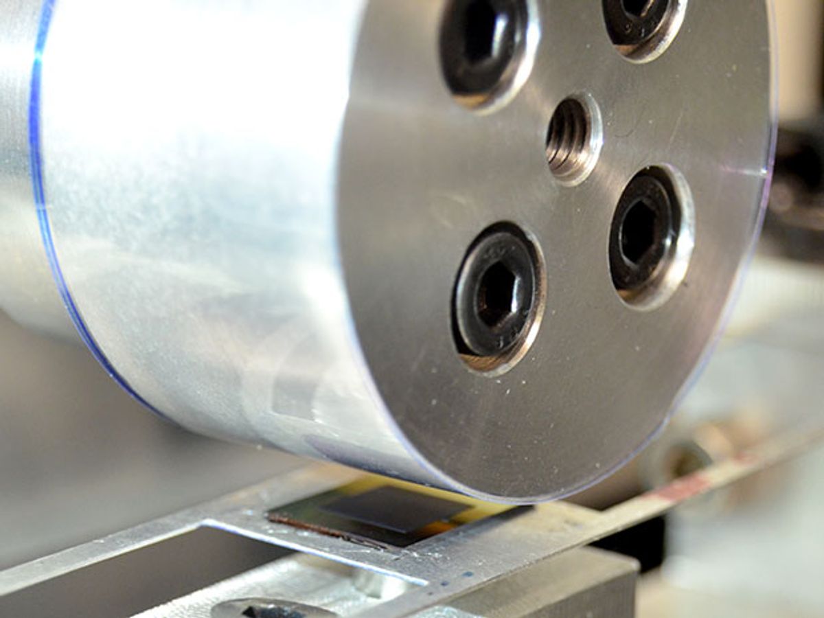
The MIT researchers have already taken steps to ramp up the speed of the production process by developing a printing machine featuring a motorized roller. The setup involved just putting various stamps onto a platform attached to a spring that allowed the researchers to control the amount of force that was being applied.
“This would be a continuous industrial process, where you would have a stamp, and a roller on which you'd have a substrate you want to print on, like a spool of plastic film or specialized paper for electronics,” Hart added. “We found [that], limited by the motor we used in the printing system, we could print at 200 millimeters per second, continuously, which is already competitive with the rates of industrial printing technologies. This, combined with a tenfold improvement in the printing resolution that we demonstrated, is encouraging.”
The end product looked to be of good quality too, according to the researchers. After annealing the electronic patterns, the researchers measured good conductivity across the printed patterns, at least good enough to serve as high-performance transparent electrodes.
Good quality and fast production are all important. But it remains to be seen whether the cost of this production process will be low enough to make sense for applications such as packaging featuring sensors that will tell you if your meat has gone bad.
Dexter Johnson is a contributing editor at IEEE Spectrum, with a focus on nanotechnology.


