- Today's microscopes don't get down to the nanoscale reliably enough for researchers who want to study objects at the atomic level.
- The nanoscale is at one billionth of a meter.
- A team of researchers from Nanyang Technological University in Singapore have created a new "nano ruler" that can measure down to 1/4,000 the wavelength of light.
Nanotechnology, which is developed at the impossibly small size of one billionth of a meter, is essential to everything from more powerful chips in smartphones to finding cures for the worst diseases. When you're that tiny, though, it's hard to measure distances. And in many cases, inventing at the nano scale means relying on indirect measurements—until now.
Researchers from Nanyang Technological University in Singapore have developed an optical ruler that uses light to measure all the way down to the nanoscale. It wasn't a cinch, though.
Given that optic devices rely on light waves, the properties of light are at the center of engineering problems that researchers may encounter. Specifically, there's the issue of limited "resolving power," which is the ability of an electronic device to produce distinguishable images. The smallest distance that can be seen through devices such as a microscope is equal to half the wavelength of the light used. This is known as the "diffraction limit."
Near infrared microscopy gets down to smaller images, so it has been regarded as a better way to measure compared to regular microscopes. It's used to identify and type gemstones, including diamonds and emeralds. Since near infrared light is at about 800 nanometers, the diffraction limit is above 400 nanometers in these microscopes. That's about 250 times smaller than the width of your hair, which is approximately 100 microns thick.
However, scientists working at the nanoscale want to observe small objects like viruses, which can range from 10 to 100 nanometers in size, rendering that optical resolution of 400 nanometers insufficient.
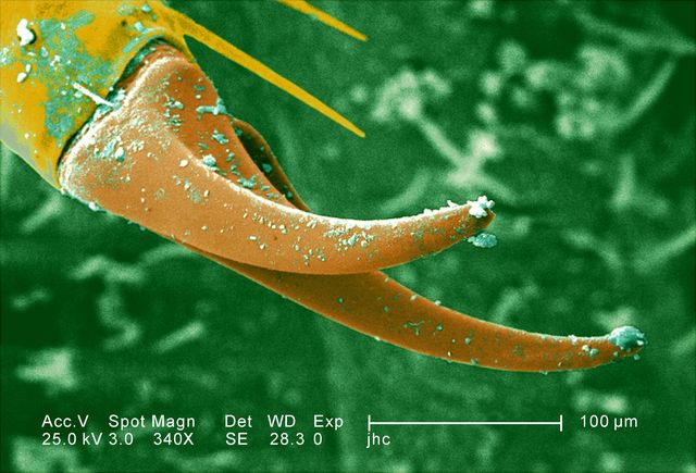
The state-of-the-art in nanometer-scale measurements has been based on indirect or downright non-optical methods, like scanning electron microscopy (SEM). SEM uses a focused beam of electrons, which interact with the atoms in a given sample, producing signals that tell about its surface and composition. (The image at the top of this article, of a doodlebug, was taken by a scanning electron microscope at a magnification of 340x.) Full-size SEMs can achieve a resolution of one to 20 nanometers.
Those devices can be difficult to get your hands on, time-consuming, and costly. Fortunately, the team at Nanyang Technological University found a solution, which has been published in the journal Science.
The new method can measure displacements of a nanometer, which is the smallest distance ever directly measured using infrared light. In theory, based on the scientist's calculations, this optical ruler can measure down to 1/4,000 of the wavelength of light, which is roughly the size of a single atom.
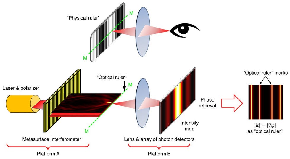
To create the "nano ruler," the team used a 100-nanometer-thick gold film with over 10,000 tiny slits etched into it to diffract laser light and take advantage of an optical phenomenon known as superoscillation, a concept that dates back to the 1980s.
Superoscillation occurs when a "sub-wavelength" in a light wave oscillates faster than the light wave itself. So long, diffraction limit.
"What makes it work is the precise pattern in which the slits are arranged," Dr. Guanghui Yuan, a postdoctoral fellow at the Centre for Disruptive Photonic Technologies center at NTU Singapore, said in a press statement. "There are two types of slits within the pattern, oriented at right angles to each other. When polarized laser light strikes the gold film, it creates an interference pattern containing extremely tiny features, much smaller than the wavelength of light."
The ruler will be a tool in manufacturing and quality control of electronics in the future, the team said.
The scientists' next challenge? Creating a compact version of their apparatus using optical fibers and hopefully commercializing the technology for use in semiconductor fabrication and optoelectronic devices that support the telecom industry.
