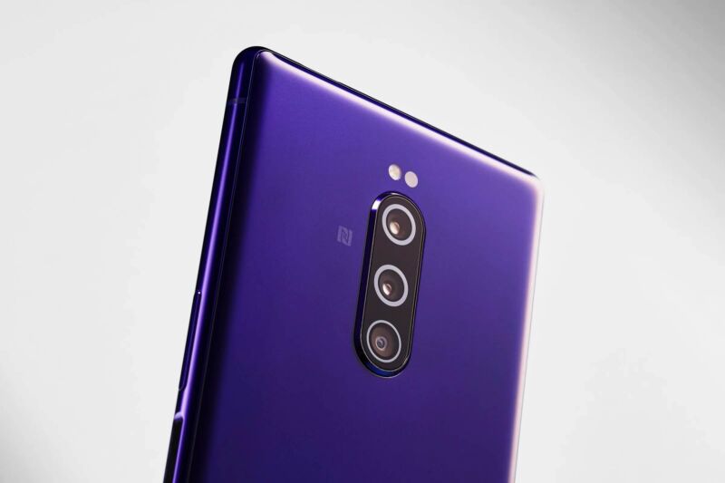
The camera on the first iPhone way back in 2007 was a mere 2 megapixels. And it only had a rear camera; there wasn't even a front-facing selfie shooter. Today, you'll find multiple cameras on the front and back of phones—some of them with sensors as large as 108 megapixels, like the biggest camera on Samsung's Galaxy S21 Ultra.
But while the sensor size and megapixel counts of smartphone cameras have increased considerably in the past decade—not to mention improvements in computational photography software—the lenses that help capture photos remain fundamentally unchanged.
![]()
A flat lens
How does it work? Well, first it's important to understand how phone camera lenses work today. The imaging system on the back of your smartphone may have multiple cameras—the latest iPhone 12 Pro has three cameras on the back—but each camera has multiple lenses or lens elements stacked on top of each other. The main camera sensor on the aforementioned iPhone 12 Pro utilizes seven lens elements. A many-lens design like the iPhone's is superior to a single-lens setup; as light passes through each successive lens, the image gains sharpness and clarity.
“The optics usually in smartphones nowadays consists of between four and seven lens elements,” says Oliver Schindelbeck, innovation manager at the optics manufacturer Zeiss, which is known for its high-quality lenses. “If you have a single lens element, just by physics you will have aberrations like distortion or dispersion in the image.”
More lenses allow manufacturers to compensate for irregularities like chromatic aberration (when colors appear on the fringes of an image) and lens distortion (when straight lines appear curved in a photo). However, stacking multiple lens elements on top of each other requires more vertical space inside the camera module. It's one of many reasons why the camera “bump” on smartphones has grown larger and larger over the years.
“The more lens elements you want to pack in a camera, the more space it needs,” Schindelbeck says. Other reasons for the size of the bump include larger image sensors and more cameras with zoom lenses, which need extra room.
Phone makers like Apple have increased the number of lens elements over time, and while some, like Samsung, are now folding optics to create “periscope” lenses for greater zoom capabilities, companies have generally stuck with the tried-and-true stacked lens element system.
“The optics became more sophisticated, you added more lens elements, you created strong aspheric elements to achieve the necessary reduction in space, but there was no revolution in the past 10 years in this field,” Schindelbeck says.
Introducing Metalenz
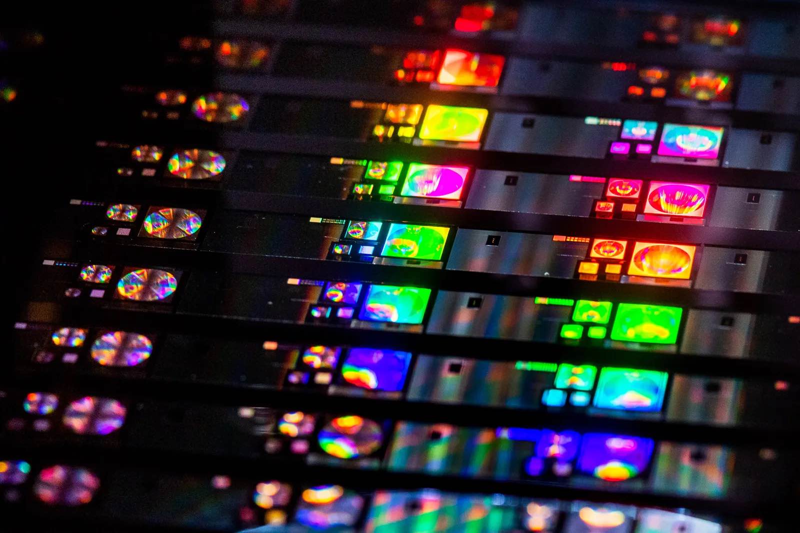
This is where Metalenz comes in. Instead of using plastic and glass lens elements stacked over an image sensor, Metalenz's design uses a single lens built on a glass wafer that is between 1x1 to 3x3 millimeter in size. Look very closely under a microscope and you'll see nanostructures measuring one-thousandth the width of a human hair. Those nanostructures bend light rays in a way that corrects for many of the shortcomings of single-lens camera systems.
The core technology was formed through a decade of research when co-founder and CEO Robert Devlin was working on his Ph.D. at Harvard University with acclaimed physicist and Metalenz co-founder Federico Capasso. The company was spun out of the research group in 2017.
Light passes through these patterned nanostructures, which look like millions of circles with differing diameters at the microscopic level. “Much in the way that a curved lens speeds up and slows down light to bend it, each one of these allows us to do the same thing, so we can bend and shape light just by changing the diameters of these circles,” Devlin says.

The resulting image quality is just as sharp as what you'd get from a multilens system, and the nanostructures do the job of reducing or eliminating many of the image-degrading aberrations common to traditional cameras. And the design doesn't just conserve space. Devlin says a Metalenz camera can deliver more light back to the image sensor, allowing for brighter and sharper images than what you'd get with traditional lens elements.
Another benefit? The company has formed partnerships with two semiconductor leaders (that can currently produce a million Metalenz "chips" a day), meaning the optics are made in the same foundries that manufacture consumer and industrial devices—an important step in simplifying the supply chain.
New forms of sensing
Metalenz will go into mass production toward the end of the year. Its first application will be to serve as the lens system of a 3D sensor in a smartphone. (The company did not give the name of the phone maker.)
Devlin says current 3D sensors, like Apple's TrueDepth camera for Face ID, actively illuminate a scene with lasers to scan faces, but this can be a drain on a phone's battery life. Since Metalenz can bring in more light to the image sensor, he claims it can help conserve power.
Other good news? If it's a 3D sensor on the front of a phone for face authentication, Devlin says the Metalenz system can eliminate the need for a bulky camera notch jutting into the screen, like the one in current iPhones. The amount of space saved by forgoing traditional lens elements will enable more phone makers to put sensors and cameras beneath a device's glass display, something we'll see more of this year.
Devlin says the applications for Metalenz reach beyond smartphones. The technology can be used in everything from instruments for health care to augmented- and virtual-reality cameras, to the cameras in automobiles.
Take spectroscopy as an example. A spectrometer is used to finely detect different wavelengths of light, and it's commonly employed in medical assays to identify particular molecules in the blood. As metasurfaces allow you to collapse “a tabletop of optics into a single surface,” Devlin claims you can pop the right sensors in a smartphone with Metalenz to do the same kind of work.
“You can actually look at the chemical signature of fruit with a spectrometer and tell whether it's ripe,” Devlin says. “It's really not just an image anymore, you're actually accessing all sorts of different forms of sense, and seeing and interacting with the world, getting a whole new set of information into the cellphone.”
This story originally appeared on wired.com.
Reader Comments (226)
View comments on forumLoading comments...