
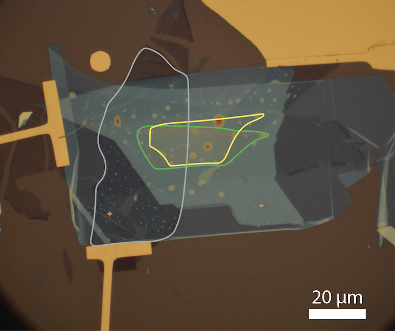
Microscope image of the TMD moiré superlattice device. (Credit: Emma Regan/Berkeley Lab)
A team of scientists led by the Department of Energy’s Lawrence Berkeley National Laboratory (Berkeley Lab) and UC Berkeley has demonstrated a powerful new technique that uses light to measure how electrons move and interact within materials. With this technique, the researchers observed exotic states of matter in stacks of atomically thin semiconductors called transition metal dichalcogenide (TMD) moiré superlattices.
Their study, which was published in the journal Nature, is the first to prove that interactions between electrons play a significant role in how charge flows in TMD moiré superlattices.
“Moiré superlattices provide a unique method for introducing exotic electronic behavior in materials where they don’t typically exist,” said lead author Emma Regan, a doctoral researcher in Berkeley Lab’s Materials Sciences Division and the UC Berkeley physics department. “Understanding and engineering electronic behavior in quantum materials may provide new approaches for electronic devices in the future.”
In most materials, electrons move fast and rarely interact. But in previous studies, other researchers have shown that a moiré superlattice – which creates an energy landscape for electrons – can slow the electrons down enough that they feel interactions between each other.
“We suspected that these electron-electron interactions in TMD moiré superlattices are very strong – even stronger than what you would find in stacks of graphene,” said Regan.
Typically, physicists investigate electron-electron interactions by attaching wires to a material and measuring how easily electrical current flows. But in stacks of TMDs, electrons don’t flow easily between the wires and the material, which makes it difficult to understand how the electrons interact.
So the researchers turned to light instead.
The research team, led by senior author Feng Wang, fabricated the TMD moiré superlattice from atomically thin layers of tungsten diselenide and tungsten disulfide – two common semiconductors known for their ability to efficiently absorb and emit light. They then formed a device just 25 nanometers (25 billionths of a meter) thick by sandwiching the tungsten diselenide/tungsten disulfide moiré superlattice between boron nitride and graphene.
In Wang’s ultrafast nano-optics lab, the researchers shone lasers on the TMD device to observe how electrons flowed in the superlattice as they varied the number of electrons injected into the material. Wang is a faculty scientist in Berkeley Lab’s Materials Sciences Division and professor of physics at UC Berkeley.
Using light to choreograph electron spin
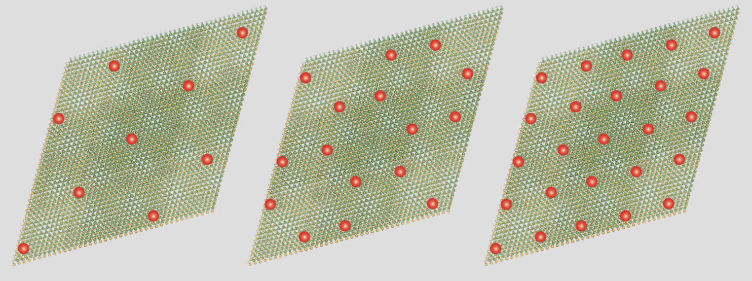
Electrons resting in the moire superlattice at different electron densities. Wigner crystal states are shown left and center. Typical insulating state is shown right. (Credit: Emma Regan/Berkeley Lab)
As expected, the researchers uncovered evidence of very strong electron-electron interactions in the TMD moiré superlattice device.
In one experiment, for example, the device suddenly became electrically insulating – the electrons stopped moving – when they added enough electrons to fill each unit cell in the moiré superlattice.
This behavior is common in a material with strong electron-electron interactions, Regan said. “Since the electrons interact strongly, they prefer not to sit at the same position because this will increase their energy. If all of the unit cells are already occupied, then the electrons stop moving around,” she explained.
So Regan and co-authors were surprised to see similar insulating behavior in the TMD moiré superlattice device when there were fewer electrons in the material, and not all the superlattice unit cells were occupied.
“Electron interactions were so strong in the TMD moiré superlattice that electrons also avoided sitting on neighboring sites,” she said. “These states are called generalized Wigner crystal states and haven’t been seen in any other moiré superlattice system.”
TMDs have a unique property where different polarizations of light can excite electrons to spin up or spin down, so the researchers used a laser to inject electrons with “spin up” or “spin down” into the material, probing their behavior with a second laser. “Direct optical access to the electron spin is special because it helps us understand the details of these exotic states,” Regan said.
“This study is very exciting because we were able to demonstrate strong electron-electron interactions in TMD moiré superlattices, which also have fascinating and useful optical properties,” she added. “This work weds traditional correlated electron physics with 2D TMD materials – two communities that usually don’t overlap.”
The researchers hope to further develop their technique to take optical measurements of electron spin at tiny scales of distance and timing.
Researchers from the Kavli Institute at Cornell for Nanoscale Science; Huazhong University of Science and Technology, and the University of the Chinese Academy of Sciences, China; Arizona State University; Lund University, Sweden; and the National Institute for Materials Science, Japan, also contributed to the study.
The work was supported by the DOE Office of Science. Additional funding was provided by the U.S. Army Research Office.
Learn more:
When Semiconductors Stick Together, Materials Go Quantum
###
Founded in 1931 on the belief that the biggest scientific challenges are best addressed by teams, Lawrence Berkeley National Laboratory and its scientists have been recognized with 13 Nobel Prizes. Today, Berkeley Lab researchers develop sustainable energy and environmental solutions, create useful new materials, advance the frontiers of computing, and probe the mysteries of life, matter, and the universe. Scientists from around the world rely on the Lab’s facilities for their own discovery science. Berkeley Lab is a multiprogram national laboratory, managed by the University of California for the U.S. Department of Energy’s Office of Science.
DOE’s Office of Science is the single largest supporter of basic research in the physical sciences in the United States, and is working to address some of the most pressing challenges of our time. For more information, please visit energy.gov/science.