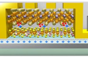
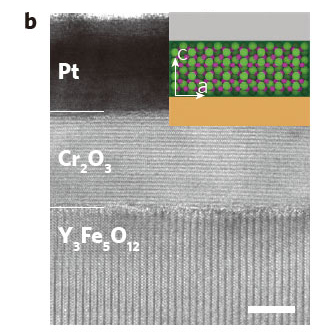
The device has a three layer structure, which sandwiches a chrome oxide (Cr2O3) layer between yttrium iron garnet (YIG) and platinum (Pt).
The YIG/Pt pair is a standard combination of materials used to investigate the current flow – both are insulators, blocking electron flow.
YIG, a ferrimagnet electric insulator, generates spin current in response to microwaves (spin pumping) or temperature gradient (spin Seebeck effect) and Pt, a paramagnetic metal, detects the spin current as an electric voltage via the inverse spin hall effect (ISHE) – which changes spin current from elsewhere into electrical voltage.
With the Cr2O3 layer included, the voltage signal at the Pt reflects how the Cr2O3 layer transmit the current, allowing changes against temperature and applied magnetic field to be identified.
“We observed a massive reduction in the voltage signal when crossing the temperature at around 300K, at which point Cr2O3 changes its phase from paramagnet to anti-ferromagnet [the Neel point],” said researcher Dazhi Hou. The change of the spin current transmission is close to 5x when a magnetic field is applied – suggesting that the layered structure works as a spin current switch when crossing the Neel point of Cr2O3 or applying a magnetic field.
The work is described in the Nature Materials paper ‘Spin colossal magnetoresistance in an antiferromagnetic insulator‘.
Diagram: Illustration of the out-of-plane spin Seebeck setup for the YIG/Cr2O3/Pt trilayer device.
Photo: TEM image of the YIG/Cr2O3/Pt trilayer device – scale bar is 5nm
Both images taken from Tohoku University website, which requested they be credited to Nature Publishing Group.