Photonic synapses with low power consumption and high sensitivity
 Schematic diagram of visual perception and information transmission in human brain and corresponding artifical MoS2 synaptic device; (b) Comparison of single optical pulse width and power consumption among some synaptic devices. Credit: Compuscript Ltd")
Neuromorphic photonics/electronics is the future of ultralow energy intelligent computing and artificial intelligence (AI). In recent years, inspired by the human brain, artificial neuromorphic devices have attracted extensive attention, especially in simulating visual perception and memory storage. Because of its advantages of high bandwidth, high interference immunity, ultrafast signal transmission and lower energy consumption, neuromorphic photonic devices are expected to realize real-time response to input data. In addition, photonic synapses can realize non-contact writing strategy, which contributes to the development of wireless communication.
The use of low-dimensional materials provides an opportunity to develop complex brain-like systems and low-power memory logic computers. For example, large-scale, uniform and reproducible transition metal dichalcogenides (TMDs) show great potential for miniaturization and low-power biomimetic device applications due to their excellent charge-trapping properties and compatibility with traditional CMOS processes. The von Neumann architecture with discrete memory and processor leads to high power consumption and low efficiency of traditional computing. Therefore, the sensor-memory fusion or sensor-memory- processor integration neuromorphic architecture system can meet the increasingly developing demands of big data and AI for low power consumption and high performance devices. Artificial synaptic devices are the most important components of neuromorphic systems. The performance evaluation of synaptic devices will help to further apply them to more complex artificial neural networks (ANN).
Chemical vapor deposition (CVD)-grown TMDs inevitably introduce defects or impurities, showed a persistent photoconductivity (PPC) effect. TMDs photonic synapses integrating synaptic properties and optical detection capabilities show great advantages in neuromorphic systems for low-power visual information perception and processing as well as brain memory.
In a study published in Opto-Electronic Advances, the research Group of Optical Detection and Sensing (GODS) have reported a three-terminal photonic synapse based on the large-area, uniform multilayer MoS2 films. The reported device realized ultrashort optical pulse detection within 5 μs and ultralow power consumption about 40 aJ, which means its performance is much better than the current reported properties of photonic synapses. Moreover, it is several orders of magnitude lower than the corresponding parameters of biological synapses, indicating that the reported photonic synapse can be further used for more complex ANN. The photoconductivity of MoS2 channel grown by CVD is regulated by photostimulation signal, which enables the device to simulate short-term synaptic plasticity (STP), long-term synaptic plasticity (LTP), paired-pulse facilitation (PPF) and other synaptic properties. Therefore, the reported photonic synapse can simulate human visual perception, and the detection wavelength can be extended to near infrared light.
As the most important system of human learning, visual perception system can receive 80% of learning information from the outside. With the continuous development of AI, there is an urgent need for low-power and high sensitivity visual perception system that can effectively receive external information. In addition, with the assistant of gate voltage, this photonic synapse can simulate the classical Pavlovian conditioning and the regulation of different emotions on memory ability. For example, positive emotions enhance memory ability and negative emotions weaken memory ability. Furthermore, a significant contrast in the strength of STP and LTP based on the reported photonic synapse suggests that it can preprocess the input light signal. These results indicate that the photo-stimulation and backgate control can effectively regulate the conductivity of MoS2 channel layer by adjusting carrier trapping/detrapping processes. Moreover, the photonic synapse presented in this paper is expected to integrate sensing-memory-preprocessing capabilities, which can be used for real-time image detection and in-situ storage, and also provides the possibility to break the von Neumann bottleneck.
-
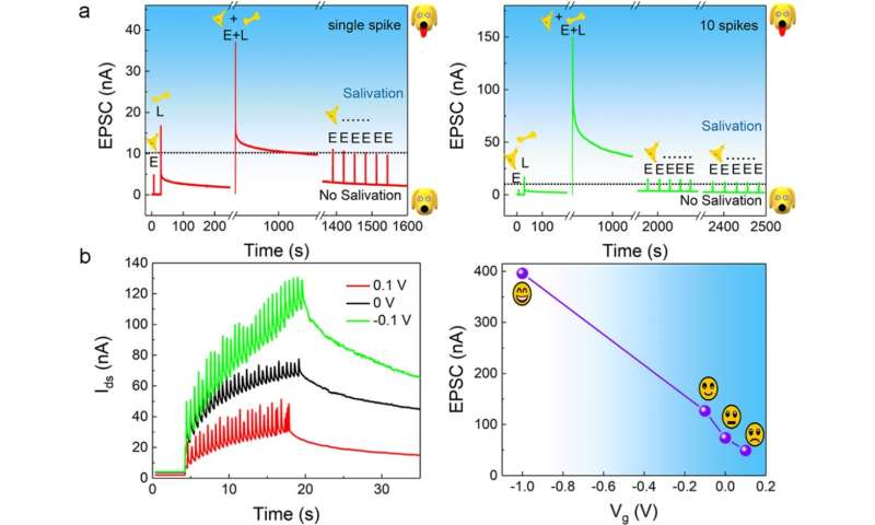
Figure 2 (a) The classical Pavlovian conditioning under one training (E+L) (left) and ten trainings (right); (b) Regulation of the device memory function via gate voltage. Credit: Compuscript Ltd -
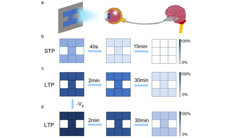
Figure 3 (a) Illustration of neuromorphic letter recognition. The stimulated letter recognition under STP (b), LTP without (c) or with (d) –Vg. Credit: Compuscript Ltd
More information: Caihong Li et al, Photonic synapses with ultralow energy consumption for artificial visual perception and brain storage, Opto-Electronic Advances (2022). DOI: 10.29026/oea.2022.210069
Provided by Compuscript Ltd


