Researchers in the US and Israel have developed a way to make 3D superconducting nanostructures by combining DNA with niobium and silicon. This new technique might be used to make signal amplifiers that enhance the speed and accuracy of quantum computers as well as ultrasensitive magnetic field sensors for medical and geophysics applications.
While traditional nanofabrication techniques like electron-beam lithography can produce one-dimensional and two-dimensional superconducting nanostructures, their ability to produce three-dimensional structures is limited. For the past 15 years or so, researchers have instead turned to self-assembly techniques that use DNA to construct 3D nanoscale structures and integrate them with functional inorganic nano-components.
One such technique, known as “DNA origami”, uses the natural pairing of DNA’s four nucleotide bases – A, T, C and G – to produce a multitude of self-assembled engineered shapes. The process involves folding a long single strand of DNA with the help of shorter complementary strands at specific locations to make pre-defined nanoscale structures. These nanostructures can then be used as scaffolding for building 3D nanoscale architectures that can be “converted” into inorganic materials such as superconductors – as in this new work, which was led by Oleg Gang, a nanoengineer at Columbia University and the Brookhaven National Laboratory’s Center for Functional Nanomaterials.
DNA origami “frames”
In their experiments, Gang and colleagues at Columbia designed octahedral-shaped DNA origami “frames” using a computer software package called caDNAno. Each edge within the frames comprises a six-helix bundle of DNA that is 28.6 nm long and contains 84 base pairs. At each end of these bundles, the researchers added a single-stranded DNA chain that measured roughly 2 nm in length and was designed to complement the DNA chain of the opposing DNA origami.
To better visualize (and subsequently characterize) the structure, the researchers inserted 10-nm-diameter gold nanoparticles into each octahedral “cage”, where the particles were held in place by a structure made from DNA that is complementary to the inner strands of the frame. The researchers then assembled the cages into a simple cubic superlattice of octahedra made from two pairs of frames and designed to have specific DNA strands targeting four complementary counterparts in-plane and two counterparts out-of-plane. The resulting superlattice samples are flakes 5-10 microns long and 1-3 microns thick, and the researchers used small angle X-ray scattering at the Brookhaven National Synchrotron Light Source II to confirm their nanoscale structure.
Mechanically robust 3D architecture
The team then solidified their ensemble by using a wet chemistry technique to coat the DNA lattices with a layer of silicon dioxide. “In its original form, DNA is completely unusable for processing with conventional nanotechnology methods,” Gang explains. “But once we coat the DNA with silica, we have a mechanically robust 3D architecture that we can deposit inorganic materials on using these methods. This is analogous to traditional nanomanufacturing, in which valuable materials are deposited onto flat substrates, typically silicon, to add functionality.”
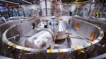
The next step was to use an evaporation technique to coat the silica-coated superlattices with a layer of niobium around 10 nm thick. This part of the work was done at the Institute of Superconductivity at Bar-Ilan University in Israel. There, researchers led by Yosi Yesurun carefully controlled both the temperature of the silicon substrate and the rate at which they deposited the niobium so that the niobium only coated the sample and did not penetrate all the way through it. They did this to prevent short circuiting between the electrodes used for later electronic transport measurements.
A periodic array of Josephson junctions
Once this step was complete, the researchers used scanning transmission microscopy with energy dispersive spectroscopy (STEM-EDS) to check the structure of their samples. This imaging technique revealed a porous superlattice structure made up of the silica-coated DNA and the gold nanoparticle “tracers”.
This structure forms a periodic array of Josephson junctions – thin non-superconducting barriers though which superconducting current tunnels – with the niobium in the superlattice being mainly confined to the top three pairs of octahedra layers (which have a total thickness of around 290 nm). As a final step, the researchers measured the current-voltage characteristics of their superlattices at temperatures between 1.9 and 3.7 K. The curves produced are typical of single Josephson junctions – that is, they show zero voltage for currents up to a certain temperature-dependent critical current (indicated by the appearance of resistance) and then a gradual voltage increase.

DNA origami produces silica ‘diatoms’
Gang and colleagues note that Josephson junctions are key components for leveraging quantum phenomena in practical technologies, with examples including the superconducting quantum interreference devices (SQUIDs) used to sense magnetic fields. The three-dimensional nature of the Josephson junctions created in this work means that more of them can be packed into the same small volume, which could increase the power of a device that uses them.
While DNA is not necessarily the most useful functional material for such work, the researchers say they have demonstrated that complex DNA organization can, in principle, be used to create highly nanostructured 3D superconducting materials. “This material conversion pathway gives us an ability to make a variety of systems with interesting properties – not only superconductivity but also other electronic, mechanical, optical, and catalytic properties,” they report. “We can envision it as a ‘molecular lithography’, where the power of DNA programmability is transferred to 3D inorganic nanofabrication.”
Spurred on by this possibility, the researchers, who report their work in Nature Communications, say they are now planning to apply the same strategy to create highly-structured 3D inorganic nanomaterials with a broad range of functions.