Researchers in China and Singapore say they have made the first ever 3D photonic topological insulator using a stack of thin plastic sheets embedded with metal nanoantennas. The insulator works at microwave frequencies, but if extended to terahertz or optical wavelengths, it could find use in applications such as high-power lasers, optical diodes and photonic computer chips.
2D topological insulators, also known as 2D quantum spin Hall insulators, are materials that are electrical insulators in the bulk but can conduct electricity extremely well on their edge via special, topologically protected, electronic states. Electrons can only travel in one direction along these states and do not backscatter. This means that they can carry electrical current with near-zero dissipation of energy and so could be used to make energy-efficient electronic devices in the future.
Structures made from photonic crystals
In recent years, researchers have started looking at making topological insulators that work using light rather than electric currents. These structures are made from photonic crystals – materials in which the periodic variation of the refractive index means that only certain wavelengths of light are able to pass through. One of the advantages of these photonic topological insulators is that they can operate at room temperature, unlike their electronic counterparts.
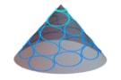
Another is that the space through which photons can travel can be engineered so that it is curved like the surface of a cone. These structures thus mimic a 2D quantum spin Hall insulator that naturally contains so-called surface Dirac cones. These are the sharp single points in a 2D material at which the valence and the conduction bands meet at the Fermi level, and at which electrons behave as though they are relativistic particles with no rest mass.
Until now, however, researchers have only been able to make 2D photonic topological insulators, and despite much theoretical work over the years 3D versions have remained elusive. Such insulators are qualitatively different from the 2D versions. Whereas 2D photonic topological insulators host topologically protected one-way edge states, 3D photonic topological insulators exhibit topological surface states that are not unidirectional. Indeed, they should be able to channel topological surface states along all possible spatial directions and not just along the planar direction.
Conventional printed circuit board technology
The new 3D topological photonic insulators were made by a team from Zhejiang University (ZJU) in China and Nanyang Technological University (NTU) in Singapore using conventional printed circuit board technology. “In our experiment, we etched dielectric laminate sheets with double-sided copper cladding,” explains study lead author Yihao Yang. “Each printed layer is paired with a dielectric spacer.”
The sheets are embedded with metal nanoantennas acting as split-ring resonators. The researchers succeeded in tailoring the resonators so that they interact with electromagnetic waves in a specific way, which allows them to give the structures the topological characteristics they require.
“The 3D photonic topological insulators have unit cells consisting of three connected metallic split-ring resonators,” says Yang. “Each is formed by arranging the unit cells in a triangular lattice in the x-y plane, and stacking identical layers along the z-direction.”
To confirm that the structure was indeed a 3D topological insulator, the researchers constructed detailed maps of how electromagnetic waves travel through it. “We did this by inserting an electromagnetic field probe into the structure and measuring the field distributions inside it and at domain walls. We then applied a Fourier transform to obtain the bulk and surface dispersion of the field distributions respectively. The latter are the physical tell-tale signatures of 3D topological insulators,” says Yang.
Extremely wide 3D topological bandgap
The researchers found that the 3D photonic topological insulators have an extremely wide 3D topological bandgap as well as gapless Dirac-cone-like topological states on their surface. “Such a wide bandgap, which exceeds even the widest ever demonstrated in 2D photonic topological insulators, will be important for future applications,” says co-team leader Hongsheng Chen of ZJU.
“On a fundamental level, we have made the first 3D topological insulator phase for bosons (photons),” says co-team leader Baile Zhang of NTU. “Because of the fundamental differences between fermions and bosons, whether a 3D bosonic photonic topological insulator could be realized was still an open question prior to our work,” he tells Physics World.
“From a technology viewpoint, such a topological insulator may be used in advanced photonic applications, such as topological photonic cavities, circuits and lasers, in previously inaccessible 3D geometries.”
Measuring local invariants in topological materials
The universality of physics
The new 3D structures are also a good example of the universality of physics, adds co-team leader Yidong Chong of NTU.“A phenomenon arising in one setting, like quantum materials, can be reproduced in another setting, in this case an artificial medium for electromagnetic waves,” he explains. “The key ingredient is that they obey the same equations and theoretical concepts.” Indeed, Chong suggests that the 3D photonic topological insulator could make for an interesting platform in which to study fundamental physics since the topological surface states are governed by the same equations as massless 2D electrons that obey Einstein’s theory of relativity.
The 3D photonic topological insulators made in this work, which is detailed in Nature 10.1038/s41586-018-0829-0, is currently limited to microwave wavelengths, but its design principles should be applicable to other frequencies, such as the terahertz or optical. The researchers say they are now busy looking into making structures that work at these frequencies.
“The present study also focused on a photonic crystal for electromagnetic waves, but a similar lattice design might be extended to other bosonic systems, such as acoustic and even mechanical structures,” says Chong.