Sponsored by Mo-SciMar 27 2024Reviewed by Louis Castel
In the rapidly evolving semiconductor manufacturing industry, where accuracy and dependability are crucial, selecting the right passivation material is essential for maximizing the performance of electronic devices. With its distinctive properties and adaptability, glass stands out among various potential materials. This article explores the use of glass for passivation and examines the characteristics that make it exceptionally well-suited for this purpose.
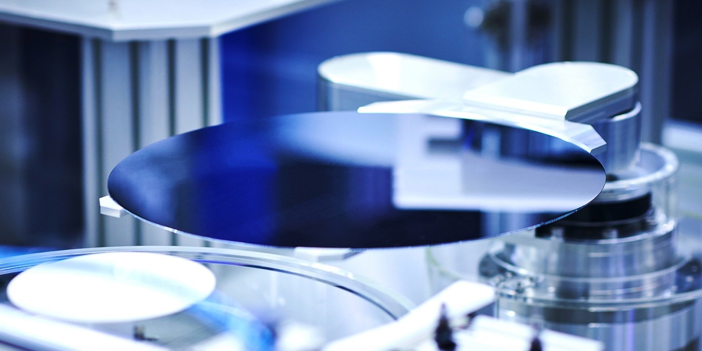
Robotic arm holding a silicon wafer for semiconductor processing. Image Credit: iStock.
Understanding Passivation in Semiconductors
Understanding the passivation process in semiconductor manufacturing is essential before unpacking the specifics of glass as a material. Passivation involves applying a protective layer to the surface of metals or metal alloys to increase resistance to environmental factors.
The layering material can be organic or inorganic. It should have superior electrical insulation and a strong bond to the substrate, as well as an ability to prevent the intrusion of chemical species. Passivation is vital in the prevention of degradation and in ensuring the long-term reliability of the semiconductors.1,2
Why Use Glass for Passivation?
Glass has a unique combination of attributes, making it a favorite choice for passivation. It can be formulated in many ways, with common types, including Pb-Si-Al, Zn-B-Si, and Pb-Zn-B.
Manufacturers can make glass that meets low and high-voltage electrical specifications, matches the coefficient of thermal expansion of semiconductor materials, and meets lower temperature processing requirements.3,4
Glass is chemically durable, providing an inert barrier against external elements, including moisture and contaminants that could impact the semiconductor’s performance.
The high transparency of some glass, like borosilicate glass, makes it perfect for projects with vital optical properties, such as photovoltaics. This transparency improves the efficiency of energy transmission and absorption, and the overall performance of semiconductor devices and solar cells.5,6
How are Semiconductors Passivated?
Glass can be deposited on the semiconductors using several different methods. The choice of method for passivation is dependent on several factors, including the semiconductor’s specific requirements, the passivation layer’s required attributes, and the process used to manufacture the device. There are several methods used to achieve glass passivation in semiconductor manufacturing:7
- Chemical vapor deposition (CVD), including plasma-enhanced CVD (PECVD)
- Physical vapor deposition (PVD), including E-beam deposition
- Sputter Coating
- Atomic Layer Deposition (ALD)
The process of glass passivation often uses chemical procedures that include the etching of contact windows or the electrolytic deposition of contacts. During manufacturing these procedures can compromise the integrity of the glass.
The chemical resistance of different passivation glass can vary substantially and is a vital factor in choosing the correct glass type and etching process.8
Comparing Glass to Other Materials
Other materials can be used for passivation, however, glass stands out for its extraordinary ability to remain stable over temperature, humidity, and time. Research reveals a lack of comparisons with other common passivation materials; however, general comparisons can be drawn.6
Amorphous silicon (a-Si) films used in solar cells have many advantages, including a lower deposition temperature. This contrasts with the temperatures regularly used in cell manufacturing. However, a-Si films are sensitive to additional high-temperature processes, which are often required in industrial manufacturing technology.9
AlOx passivation films can be used at lower temperatures but can be restricted by slow deposition speeds when a specific application method is used. This can create issues for high-throughput techniques, such as solar cell production.9
Polyimide, a common passivation material known for its strength and thermal stability, is vulnerable to moisture absorption. This can affect the strength and dielectric properties of the protective coating, putting the integrity of the semiconductor at risk.10
Applications of Glass Passivation
Passivation glass demonstrates exceptional performance in wafer passivation and encapsulation processes. This provides benefits to a wide range of semiconductor devices, including:8
- Thyristors
- Power transistors
- Diodes
- Rectifiers
- Varistors
Glass can be used in solar cell passivation. In a recent study, researchers developed a method to enhance borosilicate glass (BSG) passivation using higher temperatures before lowering the temperature to accommodate the metallization process. The process improved the solar cell’s efficiency.11
In another study, phosphosilicate glass (PSG) significantly improved the practical lifetime of minority carriers and the overall performance of solar cells in structures with nanocrystalline silicon and crystalline silicon.12
Mo-Sci’s Expertise in Glass Thin Films
The popularity of smart devices and advancements in the automotive and aerospace sectors will see the semiconductor passivation glass market grow consistently over the next few years.3
Mo-Sci’s expertise in the unique properties of glass allows the creation of tailored solutions that ensure the reliability and performance in numerous applications, including glass seals and glass coatings.
References and Further Reading
- Pehkonen, S.O., et al. (2018). Chapter 2 – Self-Assembly Ultrathin Film Coatings for the Mitigation of Corrosion: General Considerations. Interface Science and Technology. doi.org/10.1016/B978-0-12-813584-6.00002-8
- Lu, Q., et al. (2018). Chapter 5 – Polyimides for Electronic Applications. Advanced Polyimide Materials. doi.org/10.1016/B978-0-12-812640-0.00005-6
- Reliable Business Insights. [Online] Semiconductor Passivation Glass Market – Global Outlook and Forecast 2023-2028. Available at: https://www.reliablebusinessinsights.com/purchase/1365249?utm_campaign=2&utm_medium=cp_9&utm_source=Linkedin&utm_content=ia&utm_term=semiconductor-passivation-glass&utm_id=free (Accessed on 05 January 2024).
- Schott. [Online] Passivation Glass. Available at: https://www.schott.com/en-hr/products/passivation-glass-p1000287/technical-details (Accessed on 05 January 2024).
- Zhong, C., et al. (2022). Properties and mechanism of amorphous lead aluminosilicate passivation layers used in semiconductor devices through molecular dynamic simulation. Ceramics International. doi.org/10.1016/j.ceramint.2022.07.191
- Hansen, U., et al. (2009). Robust and Hermetic Borosilicate Glass Coatings by E-Beam Evaporation. Procedia Chemistry. doi.org/10.1016/j.proche.2009.07.019
- Korvus Technology. [Online] The Revolution of PVD Systems in Thin Film Semiconductor Production. Available at: https://korvustech.com/thin-film-semiconductor/ (Accessed on 05 January 2024).
- Schott. Technical Glasses: Physical and Technical Properties. Available at: https://www.schott.com/-/media/project/onex/shared/downloads/melting-and-hot-forming/390768-row-schott-technical-glasses-view-2020-04-14.pdf?rev=-1
- Bonilla, R.S., et al. (2017). Dielectric surface passivation for silicon solar cells: A review. Physica Status Solidi. doi.org/10.1002/pssa.201700293
- Babu, S.V., et al. (1993). Reliability of Multilayer Copper/Polyimide. Defense Technical Information Centre. Available at: https://apps.dtic.mil/sti/citations/ADA276228
- Liao, B., et al. (2021). Unlocking the potential of borosilicate glass passivation for industrial tunnel oxide passivated contact solar cells. Progress in Photovoltaics. doi.org/10.1002/pip.3519
- Imamura, K., et al. (2018). Effective passivation for nanocrystalline Si layer/crystalline Si solar cells by use of phosphosilicate glass. Solar Energy. doi.org/10.1016/j.solener.2018.04.063

This information has been sourced, reviewed and adapted from materials provided by Mo-Sci.
For more information on this source, please visit Mo-Sci.